Interposed substrate and manufacturing method thereof

a technology of interposed substrates and manufacturing methods, applied in the field of substrates, can solve the problems of high required cost and complex production process, and achieve the effect of reducing the required cost, favorable structure and electrical reliability

Active Publication Date: 2013-11-28
UNIMICRON TECH CORP
View PDF6 Cites 32 Cited by
  • Summary
  • Abstract
  • Description
  • Claims
  • Application Information

AI Technical Summary

Benefits of technology

[0008]The invention provides an interposed substrate capable of effectively reducing a manufacture cost while having a favorable structure and electrical reliability.

Problems solved by technology

Nevertheless, a material of the interposed substrate is a silicon wafer, and thus a required cost is higher.
However, the aforementioned production process is much complicated.

Method used


Image

  • Interposed substrate and manufacturing method thereof
  • Interposed substrate and manufacturing method thereof
  • Interposed substrate and manufacturing method thereof

Examples


Embodiment Construction

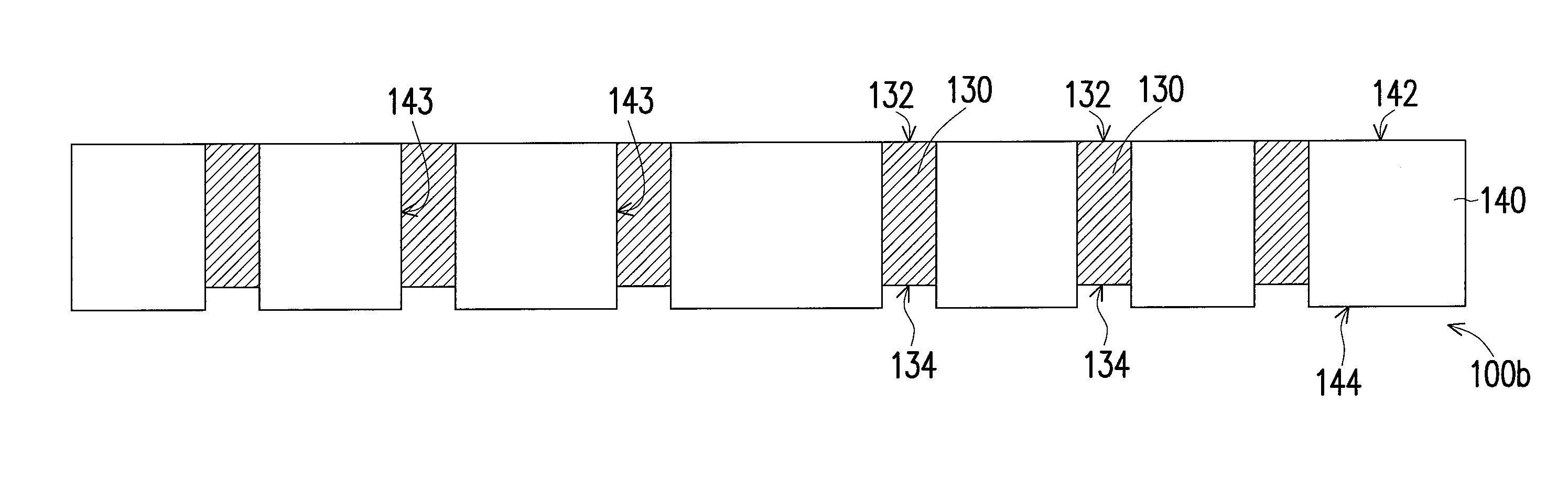
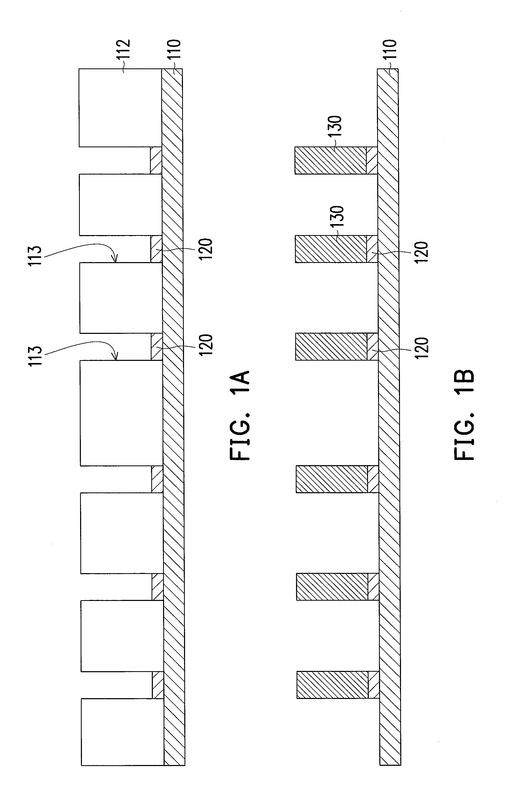
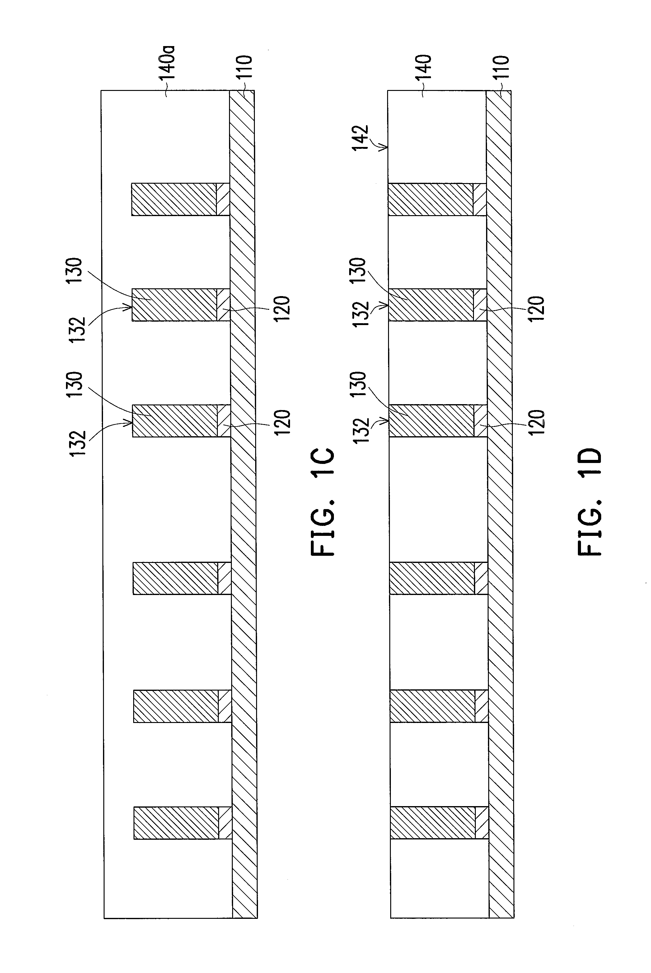
[0023]FIG. 1A to FIG. 1G are schematic cross-sectional views illustrating a manufacturing method of an interposed substrate according to an embodiment. According to the manufacturing method of the interposed substrate in the present embodiment, firstly, referring to FIG. 1A, a metal carrier 110 is provided, wherein a material of the metal carrier 110 is, for example, copper foil. Next, a photoresist layer 112 is formed on the metal carrier 110, wherein the photoresist layer 112 has a plurality of openings 113, and a portion of the metal carrier 110 is exposed by the openings 113. Then, a plurality of metal passivation pads 120 is formed in the openings 113 of the photoresist layer 112, wherein the metal passivation pads 120 cover the portion of the metal carrier 110 exposed by the openings 113. Herein, a step of forming the metal passivation pads 120 is to electroplate the metal passivation pads 120 at the portion of the metal carrier 110 exposed by the openings 113 through utilizin...


PUM

PropertyMeasurementUnit
conductiveaaaaaaaaaa
electricallyaaaaaaaaaa
densityaaaaaaaaaa

Abstract

A manufacturing method of an interposed substrate is provided. A photoresist layer is formed on a metal carrier. The photoresist layer has plural of openings exposing a portion of the metal carrier. Plural of metal passivation pads and plural of conductive pillars are formed in the openings. The metal passivation pads cover a portion of the metal carrier exposed by openings. The conductive pillars are respectively stacked on the metal passivation pads. The photoresist layer is removed to expose another portion of the metal carrier. An insulating material layer is formed on the metal carrier. The insulating material layer covers the another portion of the metal carrier and encapsulates the conductive pillars and the metal passivation pads. An upper surface of the insulating material layer and a top surface of each conductive pillar are coplanar. The metal carrier is removed to expose a lower surface of the insulating material layer.

Description

CROSS-REFERENCE TO RELATED APPLICATION[0001]This application claims the priority benefit of Taiwan application serial no. 101118578, filed on May 24, 2012. The entirety of the above-mentioned patent application is hereby incorporated by reference herein and made a part of this specification.BACKGROUND[0002]1. Field of the Invention[0003]The invention relates to a substrate and a manufacturing method thereof, and more particularly to, an interposed substrate and a manufacturing method thereof.[0004]2. Description of Related Art[0005]In the current information society, the design of electronic product is tended towards a trend of lightweight, thin, short, and compactness. As such, the development of various packaging technologies, such as the stack-type semiconductor device packaging technology, facilitates a miniaturization of the semiconductor package. In a stacked-type semiconductor device package, a plurality of semiconductor devices is vertically stacked and packaged in the same ...

Claims


Application Information

Patent Timeline
Patent Type & Authority Applications(United States)
IPC IPC(8): H05K1/11C25D5/02H05K3/10H05K3/00B23K31/02
CPCC25D1/003H05K1/113H05K3/424H05K3/4647H05K3/4682H05K2201/10378H05K2203/0152H05K2203/0733H05K2203/0726Y10T29/49155Y10T156/10H01L21/481
Inventor HU, DYI-CHUNGCHEN, MING-CHIHTSENG, TZYY-JANG
Owner UNIMICRON TECH CORP
Why Eureka
Try Eureka