Exposure apparatus and device manufacturing method

a technology of exposure apparatus and manufacturing method, which is applied in the direction of electrographic process apparatus, printing, instruments, etc., can solve the problems of disabling precise adjustment of the pattern line width error within each shot region, and the difference between the line width of the obtained pattern and that of the designed pattern, so as to improve the line width uniformity of the pattern within the shot region

Active Publication Date: 2013-11-28
CANON KK
View PDF11 Cites 6 Cited by
  • Summary
  • Abstract
  • Description
  • Claims
  • Application Information

AI Technical Summary

Benefits of technology

[0007]The present invention provides an exposure apparatus for improving the line width uniformity of a pattern within a shot region.

Problems solved by technology

Even if, however, the exposure apparatus repeatedly exposes a photoresist with a given exposure amount in each shot within a substrate plane, there is a difference (pattern line width error) between the line width of the obtained pattern and that of a designed pattern.
The conventional techniques adjust an exposure amount within the substrate plane but do not adjust an exposure amount for uniforming a line width distribution within a shot region, thereby disabling precise adjustment of a pattern line width error within each shot region.

Method used


Image

  • Exposure apparatus and device manufacturing method
  • Exposure apparatus and device manufacturing method
  • Exposure apparatus and device manufacturing method

Examples


Embodiment Construction

[0018]An embodiment of the present invention will be described in detail below with reference to the accompanying drawings.

Embodiment of Exposure Apparatus

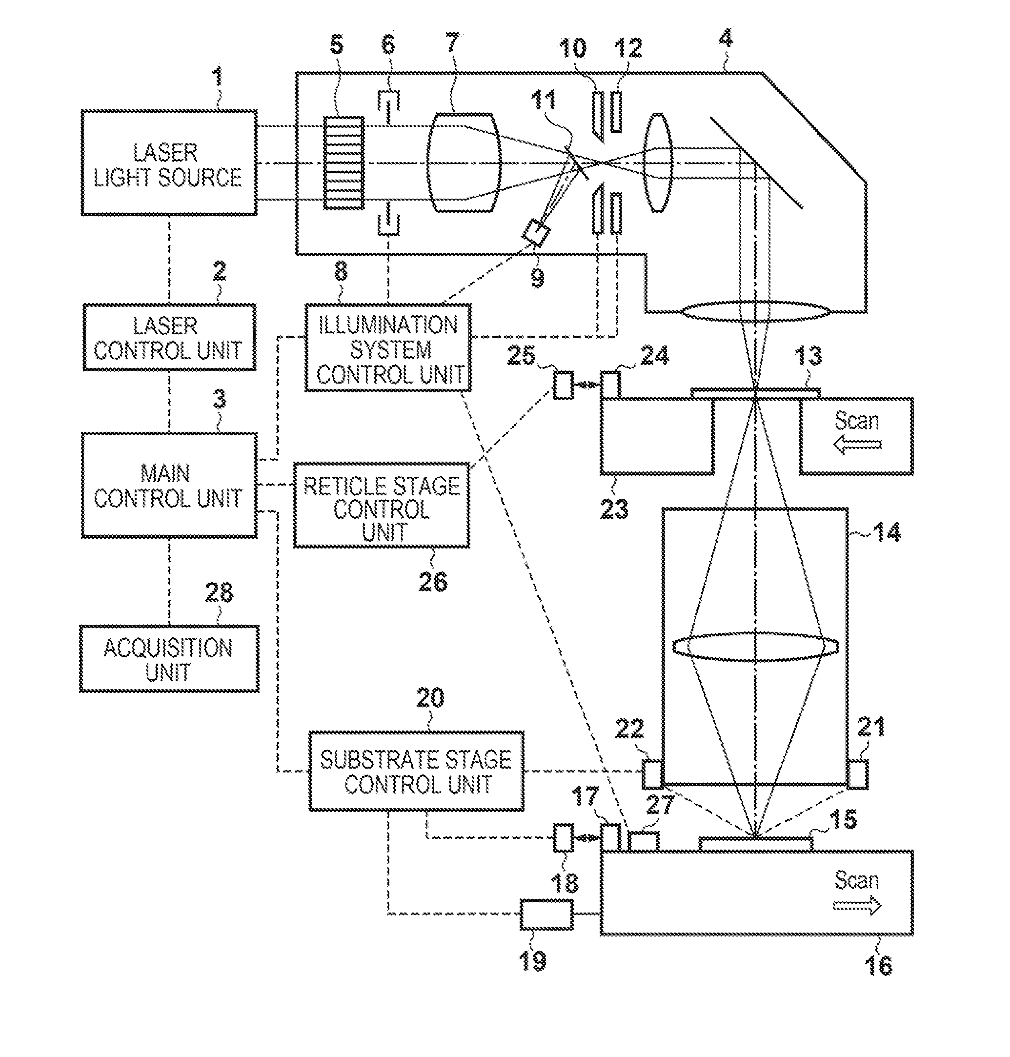
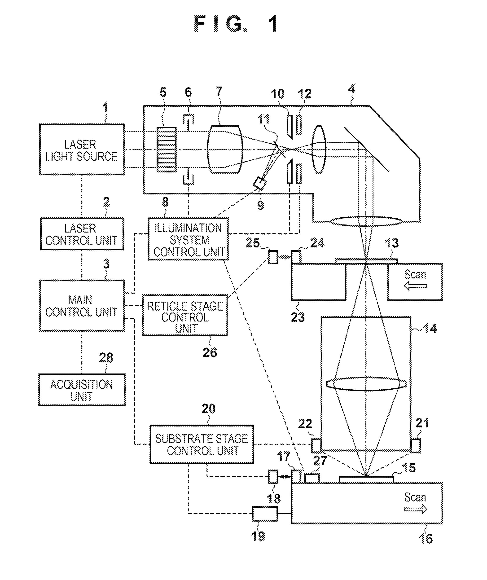
[0019]FIG. 1 shows the schematic arrangement of a step-and-scan type exposure apparatus (scan exposure apparatus) according to the embodiment of the present invention. The exposure apparatus uses slit-shaped light on an original and substrate (wafer) to scan them and expose each shot region on the substrate via the original. A laser light source 1 which is filled with, for example, ArF gas, and emits a laser beam generates light with a wavelength of 193 nm in the far-ultraviolet range. The laser light source 1 includes a front mirror forming a resonator, a band-narrowing module, a monitor module, and a shutter. The band-narrowing module includes a diffraction grating and a prism, and narrows the band of the exposure wavelength. The monitor module includes a spectroscope and a detector, and monitors the spectral width.

[0020]A laser...


PUM


Abstract

An exposure apparatus includes a control unit configured to calculate a target exposure amount distribution in a scanning direction within the target shot region using a target exposure amount at a position in the target shot region and a target exposure amount at a position in an adjacent shot region adjacent to the target shot region in the scanning direction and configured to perform a scan exposure for the target shot region while controlling an exposure amount according to scanning of the substrate so as to obtain the calculated target exposure amount distribution as an exposure amount distribution in a scanning direction within the target shot region.

Description

BACKGROUND OF THE INVENTION[0001]1. Field of the Invention[0002]The present invention relates to an exposure apparatus and a device manufacturing method.[0003]2. Description of the Related Art[0004]A process of manufacturing a semiconductor device formed from an extra fine pattern has conventionally adopted a reduction projection exposure apparatus which reduces and projects, on a substrate such as a wafer coated with a photoresist, a circuit pattern drawn on a reticle (mask), thereby exposing the substrate. Along with an improvement in the packaging density of semiconductor devices, further micropatterning of a circuit pattern is required, and an exposure apparatus which can uniform the finishing size (line width) of a pattern is desired.[0005]A conventional exposure apparatus exposes a photoresist coated on a substrate with an exposure amount (dose) corresponding to the photoresist. An exposure apparatus adopting the step-and-repeat scheme repeatedly performs an exposure with a gi...

Claims


Application Information

Patent Timeline
Patent Type & Authority Applications(United States)
IPC IPC(8): G03B27/80
CPCG03G15/043G03F7/70558G03F7/70358
Inventor KEMMOKU, HIROMI
Owner CANON KK
Why Eureka
Try Eureka