Process for large-scale ammonothermal manufacturing of semipolar gallium nitride boules

a gallium nitride boule, large-scale technology, applied in the growth process of crystals, synthetic resin layered products, polycrystalline material growth, etc., can solve the problems of poor optoelectronic device performance, difficult to provide bulk layer of gan material, and drawbacks of hvpe techniques

Active Publication Date: 2013-12-05
SLT TECH
View PDF2 Cites 39 Cited by
  • Summary
  • Abstract
  • Description
  • Claims
  • Application Information

AI Technical Summary

Benefits of technology

[0010]In a first aspect, gallium-containing nitride crystals or wafers are provided, comprising: a crystalline substrate member having a length greater than about 5 millimeters; large-area surfaces having a semipolar orientation, wherein the semipolar orientation is miscut from each of the m-plane and c-plane orientations by at least about 5 degrees; and an impurity concentration greater than about 1016 cm−3 of at least one impurity selected from O, H, Li, Na, K, F, Cl, Br, I, Cu, Mn, and Fe, wherein the at least one impurity has a distribution along a direction parallel at least one large-area surface of the crystal or wafer comprising at least 4 bands of alternating higher and lower impurity concentrations of the at least one impurity, wherein the higher impurity concentration is higher is between about 1.05 times and about 40 times the lower impurity concentration.
[0011]In a second aspect, methods for fabricating a gallium-containing nitride semipolar wafer are provided, the methods comprising: providing a gallium-containing source material; providing a mineralizer; providing a plurality of gallium-containing nitride seed plates, wherein each of the plurality of seed plates comprises a first large-area surface with a first crystallographic orientation within about 5 degrees of a growth orientation selected from

Problems solved by technology

Although successful, conventional growth rates make it difficult to provide a bulk layer of GaN material.
Additionally, dislocation densities are also high and lead to poor optoelectronic device performance.
Unfortunately, drawbacks exist with HVPE techniques.
In some cases, the quality of the bulk monocrystalline gallium nitride is not generally sufficient for high quality laser diodes because of issues with dislocation density, stress, and the like.
In addition, scale-up of HVPE is difficult and costs tend to be high, particularly for manufacturing of semipolar boules and wafers.
However, using these sup

Method used


Image

  • Process for large-scale ammonothermal manufacturing of semipolar gallium nitride boules
  • Process for large-scale ammonothermal manufacturing of semipolar gallium nitride boules
  • Process for large-scale ammonothermal manufacturing of semipolar gallium nitride boules

Examples


example 1

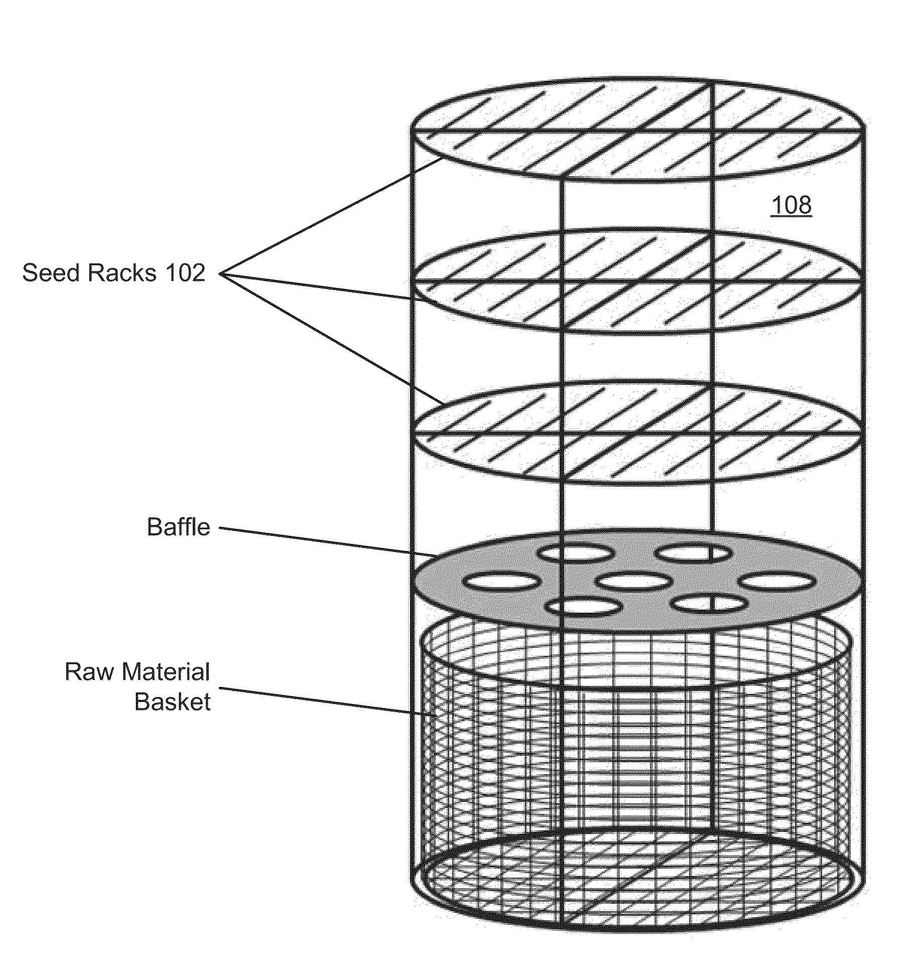
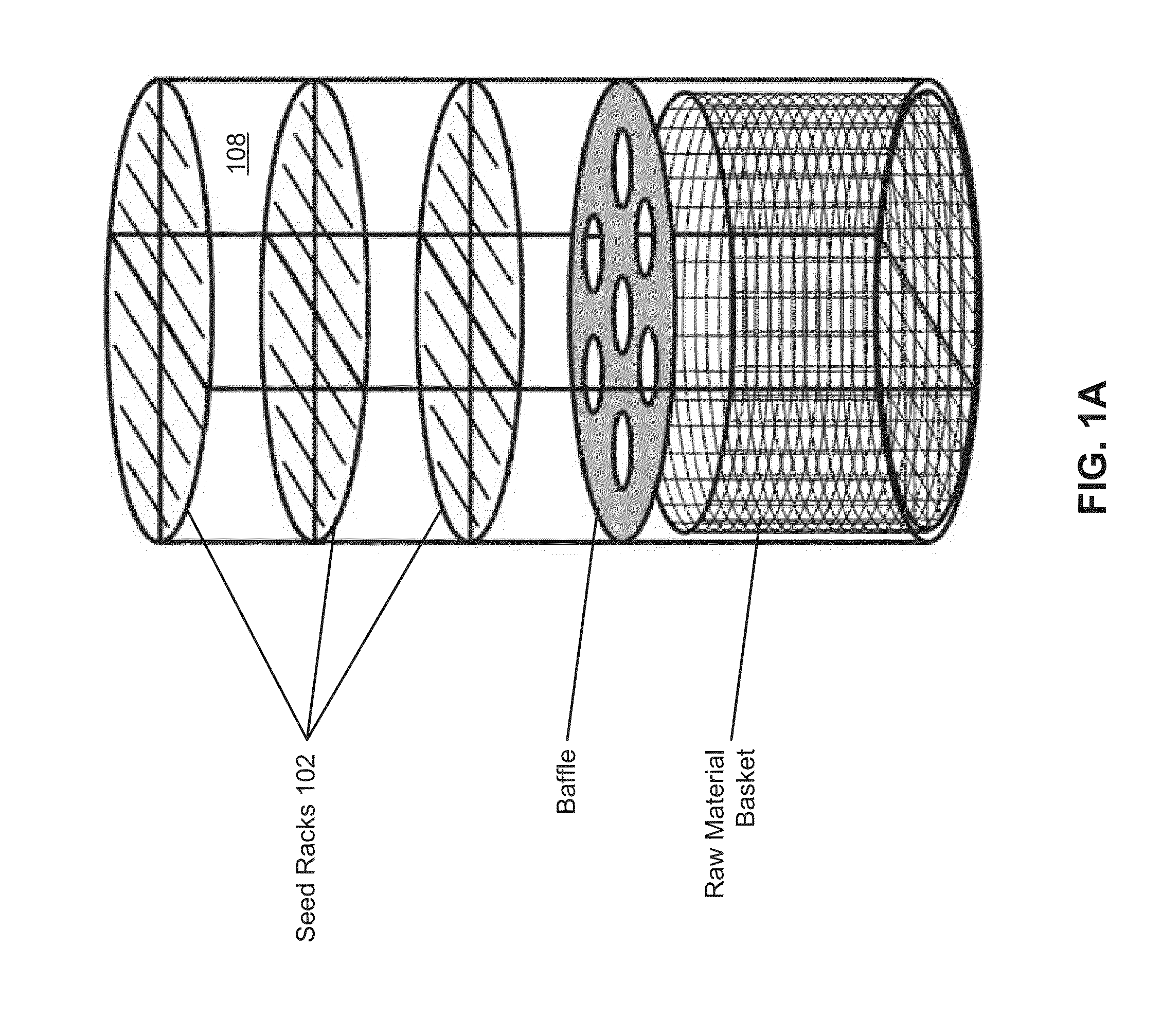
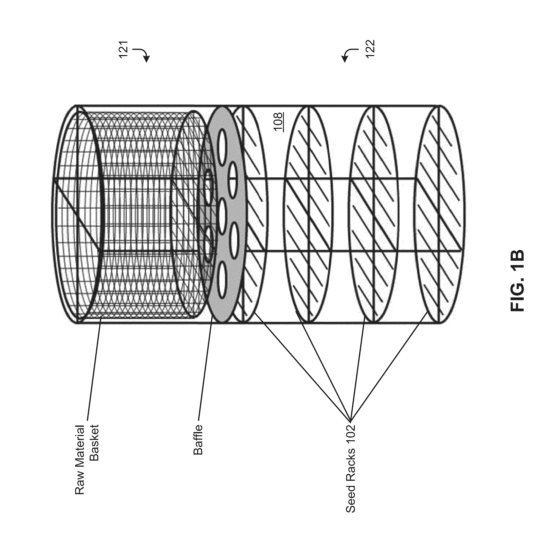
[0101]Several bulk GaN crystals grown by HVPE, approximately 0.3 millimeters thick, were provided for use as seed crystals for ammonothermal growth. A first seed crystal had a large-area surface that was miscut from the m-plane by approximately 0.03 degree toward [11-20] and by approximately 0.05 degrees toward [000−1]. A second seed crystal had a large-area surface that was miscut from the m-plane by less than 0.1 degree toward [11-20] and by approximately 1 degree toward [000−1]. A third seed crystal had a large-area surface that was miscut from m-plane by less than 0.1 degree toward [11-20] and by approximately 4 degrees toward [000−1]. A fourth seed crystal had a large-area surface that was miscut from the m-plane by less than 0.1 degree toward [11-20] and by approximately 7 degrees toward [000−1]. The seed crystals were placed inside a silver capsule along with a 15%-open-area baffle, approximately 30.6 grams of polycrystalline GaN nutrient, 5.5 grams of NH4F mineralizer, and 2...

example 2

[0106]Several bulk GaN crystals grown by HVPE, approximately 0.3 millimeters thick, were provided for use as seed crystals for ammonothermal growth. A first seed crystal had a large-area surface that was miscut from the m-plane by approximately 0.03 degree toward [11-20] and by approximately 0.05 degree toward [000−1]. A second seed crystal had a large-area surface that was miscut from m-plane by approximately 4.9 degrees toward [11-20] and by approximately 1.2 degrees toward [000−1]. A third seed crystal had a large-area surface that was miscut from m-plane by approximately 4.6 degrees toward [11-20] and by approximately 7.2 degrees toward [000−1]. The seed crystals were placed inside a silver capsule along with a 15%-open-area baffle, approximately 37.1 grams of polycrystalline GaN nutrient, 2.6 grams of NH4F mineralizer, and 29.6 grams of ammonia and the capsule was sealed. The capsule was placed in an internally-heated high pressure apparatus and heated to temperatures of approx...

example 3

[0108]Several bulk GaN crystals grown by HVPE, approximately 0.3 millimeters thick, were provided for use as seed crystals for ammonothermal growth. A first seed crystal had a large-area surface that was miscut from the m-plane by approximately 0.03 degree toward [11-20] and by approximately 0.05 degrees toward [000−1]. A second seed crystal had a large-area surface that was miscut from (10-1-1) by approximately 0.01 degree toward [−12-10] and by approximately 0.39 degrees toward [0001]. The seed crystals were placed inside a silver capsule along with a 15%-open-area baffle, approximately 36.9 grams of polycrystalline GaN nutrient, 2.7 grams of NH4F mineralizer, and 29.1 grams of ammonia and the capsule was sealed. The capsule was placed in an internally-heated high pressure apparatus and heated to temperatures of approximately 650 degrees Celsius for the upper, nutrient zone and approximately 680 degrees Celsius for the lower, crystal growth zone, maintained at these temperatures f...


PUM

PropertyMeasurementUnit
Lengthaaaaaaaaaa
Lengthaaaaaaaaaa
Lengthaaaaaaaaaa

Abstract

Methods for large-scale manufacturing of semipolar gallium nitride boules are disclosed. The disclosed methods comprise suspending large-area single crystal seed plates in a rack, placing the rack in a large diameter autoclave or internally-heated high pressure apparatus along with ammonia and a mineralizer, and growing crystals ammonothermally. A bi-faceted growth morphology may be maintained to facilitate fabrication of large area semipolar wafers without growing thick boules.

Description

[0001]This application claims the benefit under 35 U.S.C. §119(e) of U.S. Provisional Application No. 61 / 655,172, filed on Jun. 4, 2012, which is incorporated by reference in its entirety.GOVERNMENT LICENSE RIGHTS[0002]This invention was made with government support under Contract DE-SC0006168 awarded by the U.S. Department of Energy. The government has certain rights in the invention.BACKGROUND[0003]The present disclosure generally relates to processing of materials for growth of crystals. More particularly, the present disclosure provides methods for obtaining a gallium-containing nitride crystal by an ammonothermal technique, including ammonobasic or ammonoacidic techniques, but there can be others. In certain embodiments, the present disclosure provides an apparatus for large scale processing of nitride crystals, but it would be recognized that other crystals and materials may also be processed. Such crystals and materials include, for example, GaN, AN, InN, InGaN, AlGaN, AlInN,...

Claims


Application Information

Patent Timeline
IPC IPC(8): C30B29/40C30B7/10
CPCC30B29/406C30B7/105C30B19/02C30B23/04C30B25/04
Inventor D'EVELYN, MARK P.EHRENTRAUT, DIRKKAMBER, DERRICK S.DOWNEY, BRADLEY C.
Owner SLT TECH
Why Eureka
Try Eureka