Radiation detection equipment and nuclear medicine diagnosis device

a technology of radiation detection equipment and diagnosis device, which is applied in the field of radiation detection equipment and nuclear medicine diagnosis device, can solve problems such as deterioration of energy resolution, and achieve the effect of stable response performan

Inactive Publication Date: 2013-12-05
HITACHI LTD
View PDF2 Cites 14 Cited by
  • Summary
  • Abstract
  • Description
  • Claims
  • Application Information

AI Technical Summary

Benefits of technology

[0034]As mentioned hereinbefore, the present invention is capable of providing inexpensive radiation detection equipment having a sta

Problems solved by technology

Hereby, if such ions are accumulated near the anode and the cathode, that is, if charges are accumulated near the anode and the cathode (namely, if a phenomeno

Method used


Image

  • Radiation detection equipment and nuclear medicine diagnosis device
  • Radiation detection equipment and nuclear medicine diagnosis device
  • Radiation detection equipment and nuclear medicine diagnosis device

Examples


first embodiment

of Radiation Detection Equipment

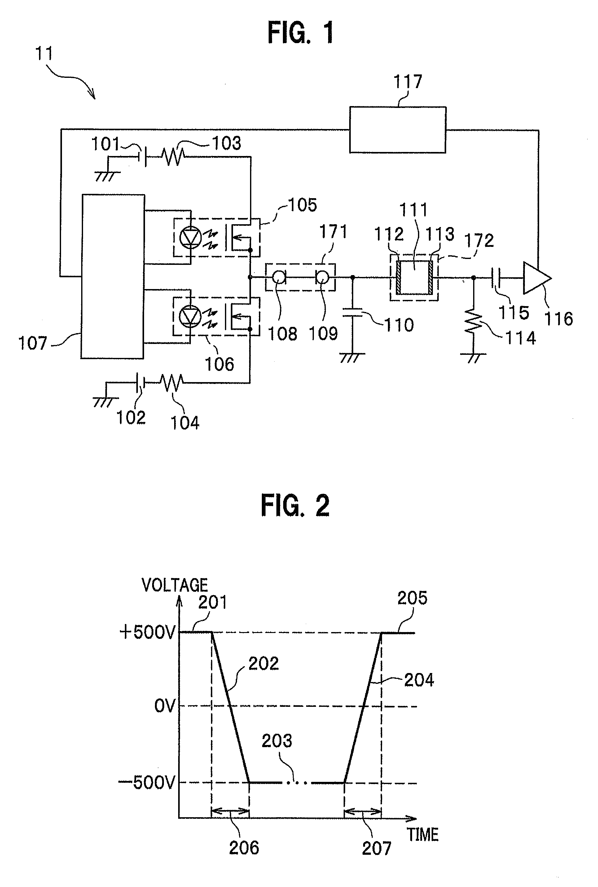
[0044]FIG. 1 is a bloc diagram showing a circuit structure of the radiation detection equipment in a first embodiment of the present invention. As shown in FIG. 1, radiation detection equipment 11 comprises: a semiconductor radiation detector (hereinafter, simply called a detector) 172 including a semiconductor crystal 111 made of thallium bromide, a first electrode 112 made of gold and a second electrode 113 also made of gold, respectively arranged at opposite surface sides of the semiconductor crystal 111; a smoothing capacitor 110 of applying a voltage to the detector 172; a first DC power source 101 of accumulating positive charges in one of electrodes of the smoothing capacitor 110; and a second DC power source 102 of accumulating negative charges in the other electrode of the smoothing capacitor 110.

[0045]The radiation detection equipment 11 further comprises: a first constant regulative diode 108 which is connected by integrating the polarity o...

second embodiment

of Radiation Detection Equipment

[0130]FIG. 4 is a bloc diagram showing a circuit structure of the radiation detection equipment in a second embodiment of the present invention. As shown in FIG. 4, radiation detection equipment 21 comprises: a semiconductor radiation detector (hereinafter, simply called a detector) 372 including a semiconductor crystal 312 made of thallium bromide, a first electrode 313 made of gold and a second electrode 314 also made of gold, respectively arranged at opposite surface sides of the semiconductor crystal 312; a smoothing capacitor 311 of applying a voltage to the detector 372; and a DC power source 301 of accumulating positive charges or negative charges in either of electrodes of the smoothing capacitor 311.

[0131]The radiation detection equipment 21 further comprises: a first constant regulative diode 309 which is connected by integrating the polarity of the constant-current characteristics so that a current flows from the DC power source 301 to eith...


PUM


Abstract

Provided is radiation detection equipment including: a semiconductor radiation detector which has a semiconductor crystal made of thallium bromide; a capacitor which applies a voltage to the semiconductor radiation detector; and at least one DC power source which accumulates positive charges and negative charges in either of electrodes of the capacitor. Herein, a cathode and an anode in the semiconductor radiation detector are formed of at least one kind of a metal selected from gold, platinum and palladium. Further, the DC power source periodically reverses a voltage of accumulating the positive charges and a voltage of accumulating the negative charges in either of the electrodes of the capacitor per interval shorter than 10 min, thereby to apply the resulting voltage thereto.

Description

BACKGROUND OF THE INVENTION[0001]1. Field of the Invention[0002]The present invention relates to radiation detection equipment and a nuclear medicine diagnosis device.[0003]2. Description of the Related Art[0004]Recently, a nuclear medicine diagnosis device using radiation detection equipment which detects radiations such as γ rays (or gamma rays) or the like has been widely spread in medical fields. A representative nuclear medicine diagnosis device includes a gamma camera device, imaging equipment for single photon emission computed tomography (SPECT), imaging equipment for positron emission tomography (PET) or the like. Further, a demand for using radiation detection equipment is increasing in a field of homeland security, in which a dosimeter using radiation detection equipment is applied to the dirty bomb counterterrorism.[0005]Conventionally, a radiation detector mounted on the above mentioned radiation detection equipment was produced by combining a scintillator (that is, a d...

Claims


Application Information

Patent Timeline
IPC IPC(8): G01T1/161A61B6/02
CPCG01T1/1618A61B6/02A61B6/037A61B6/0407A61B6/4258
Inventor KOMINAMI, SHINYA
Owner HITACHI LTD
Why Eureka
Try Eureka