

Flash charging protection circuit and control method thereof
- Summary
- Abstract
- Description
- Claims
- Application Information
AI Technical Summary
Benefits of technology
Problems solved by technology
Method used
Image

Examples
Embodiment Construction
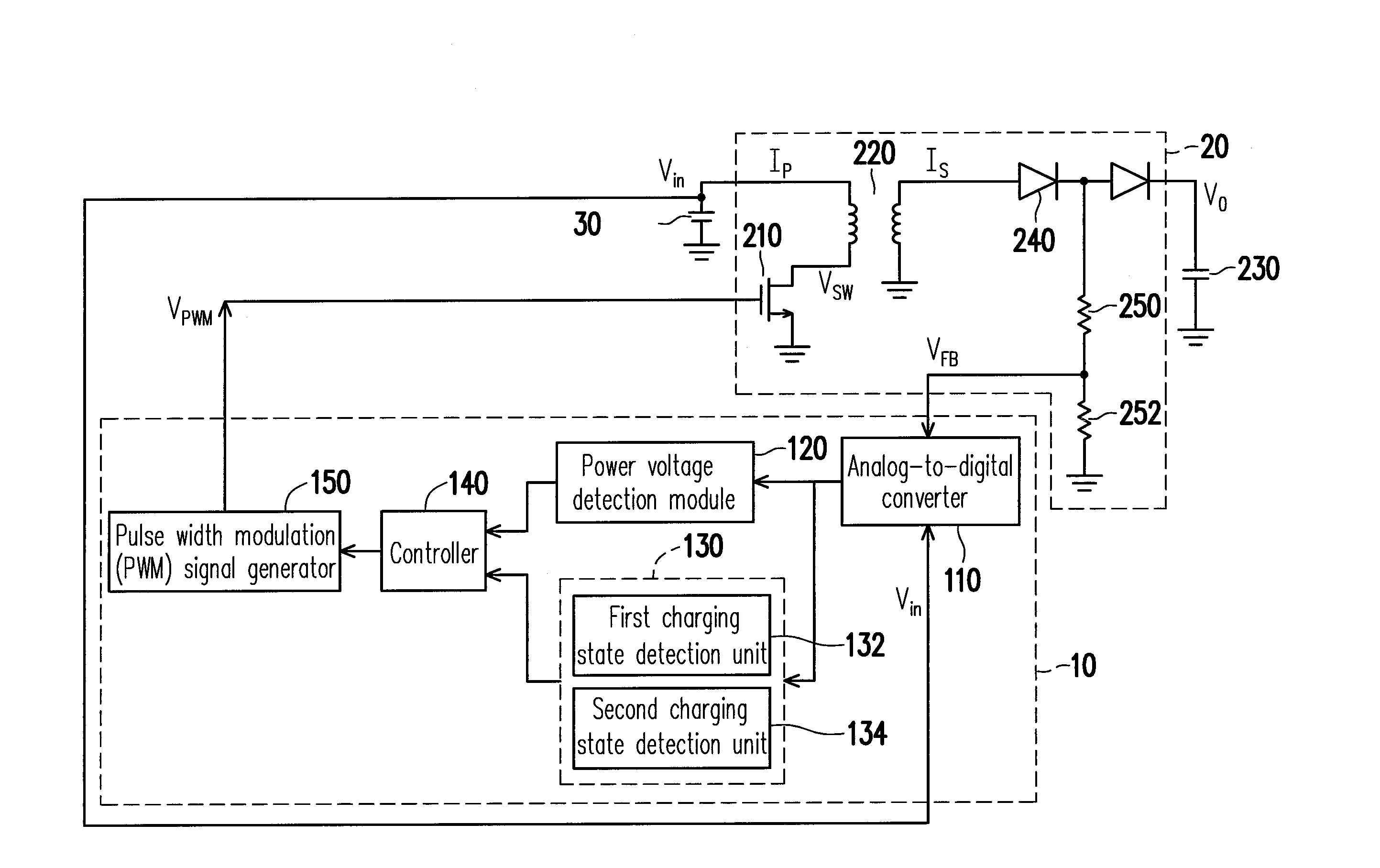
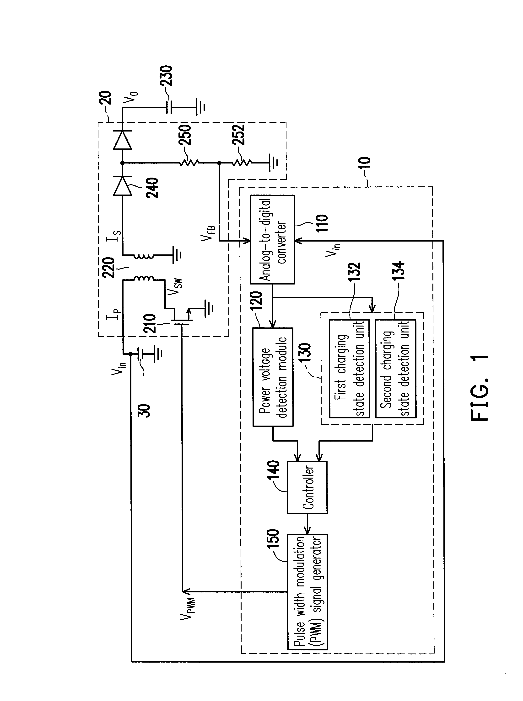
[0033]FIG. 1 is a diagram of a flash charging protection circuit according to an embodiment of the invention. Referring to FIG. 1, the flash charging protection circuit 10 is adapted to a charging circuit 20, and the charging circuit 20 includes a power switch 210 and a transformer 220, where the power switch 210 is coupled to a first side winding of the transformer 220. A power supply 30 is coupled to the first side winding of the transformer 220, and provides an input voltage Vin. The transformer 220 transforms the input voltage Vin to output an output voltage Vo through a second side winding thereof, and the output voltage Vo can be used to charge an energy storage element. In the present embodiment, the power switch 210 is, for example, a power metal oxide semiconductor field effect transistor (MOSFET), and the energy storage element is, for example, a capacitor 230. Moreover, to prevent electricity leakage of the capacitor 230 after the capacitor 230 is fully charged, at least ...
PUM
 Abstract
Description
Claims
Application Information