Semiconductor memory structure and control method thereof

Inactive Publication Date: 2014-01-02
FUDAN UNIV
View PDF4 Cites 7 Cited by
  • Summary
  • Abstract
  • Description
  • Claims
  • Application Information

AI Technical Summary

Benefits of technology

[0020]According to the method for controlling the semiconductor memory structure, the tunneling field-effect transistor is adopted to carry out operations such as erasing, writing, and reading the semiconductor memory structure, the vertical gate-controlled diode structure in the tunneling field-effect transis

Problems solved by technology

By means of the current technology, integrated circuit devices are about 30 nm; however, limited by high coupling ratios, high voltage, etc., traditio

Method used


Image

  • Semiconductor memory structure and control method thereof
  • Semiconductor memory structure and control method thereof
  • Semiconductor memory structure and control method thereof

Examples


Example

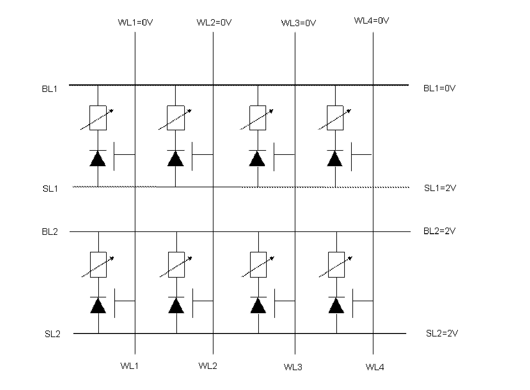
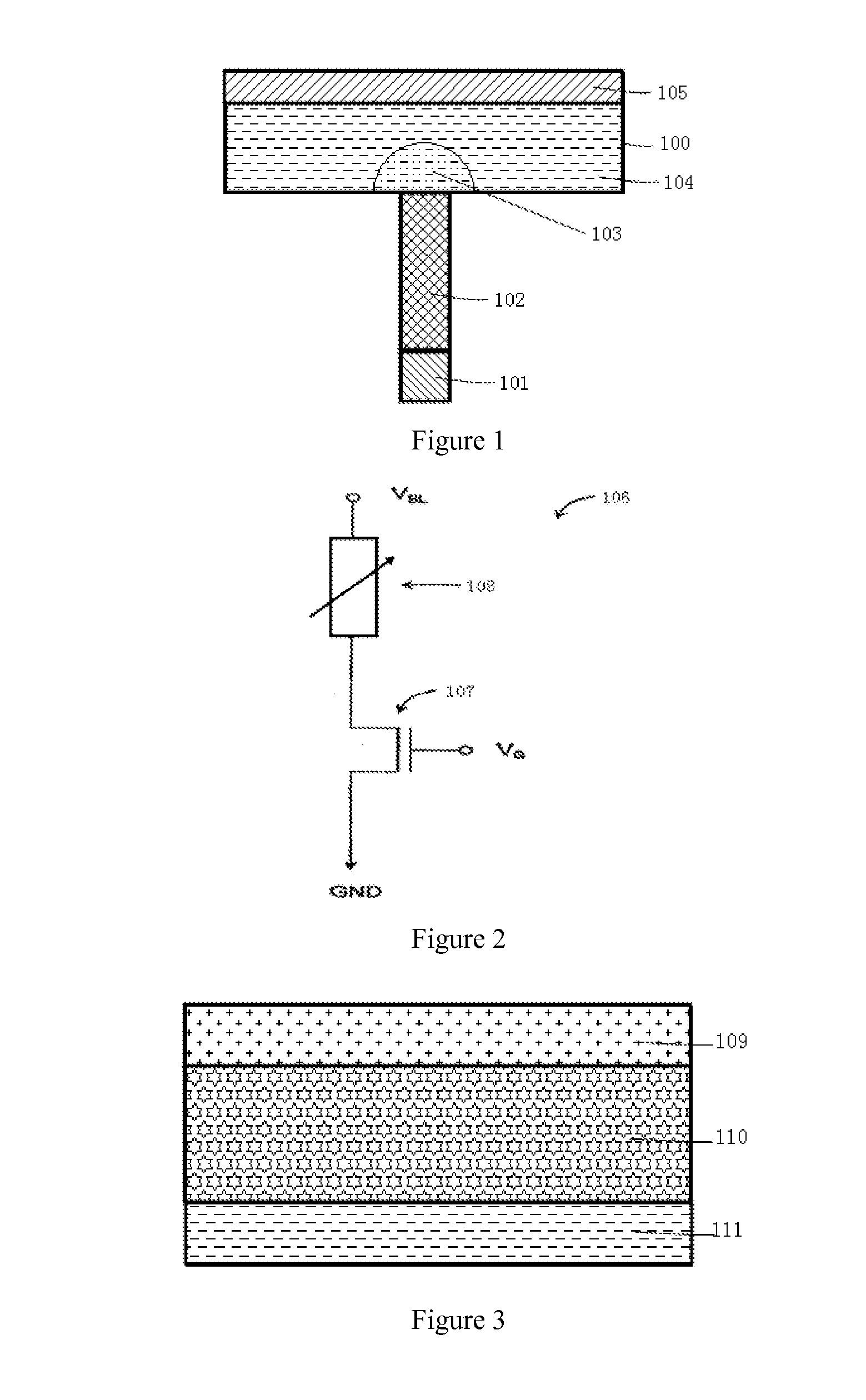
[0030]The embodiment of the present invention is further described in detail by means of the attached drawings. In the figure, to facilitate description, the layer thickness and region thickness are amplified, but the sizes do not represent the actual dimensions. The attached drawings are schematic views of an ideal embodiment. The embodiment of the present invention shall not be limited to the specific shapes of the regions as shown in the figure, but shall comprise all shapes, like deviation caused by manufacturing.

[0031]For example, an etched curve is usually characterized in bends or roundness and smoothness. But in this embodiment, all curves are represented by rectangles. The figure is schematic and shall not be considered as a limit of the present invention. Meanwhile, in the below description, the term “wafer” and “substrate” may be considered to comprise a semiconductor wafer being processed or other films prepared on the semiconductor wafer.

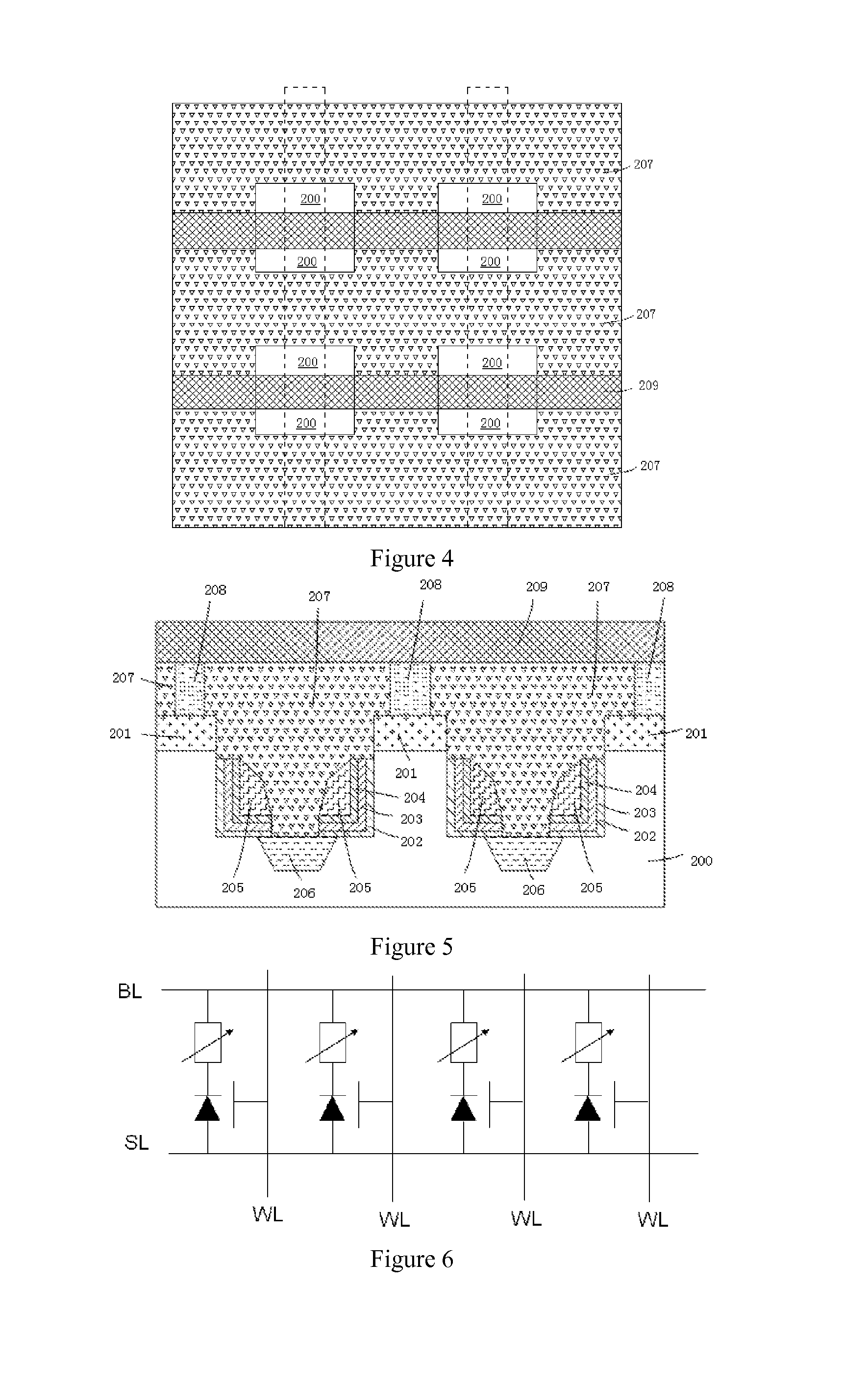
[0032]FIG. 4 is a top view of a ...


PUM


Abstract

The present invention belongs to the technical field of non-volatile semiconductor memories, and relates to a semiconductor memory structure and a control method thereof. The semiconductor memory structure in the present invention comprises a memory unit for storing information and a tunneling field-effect transistor connected with the memory unit. The tunneling field-effect transistor is used for controlling the semiconductor memory's operations such as erasing, writing, and reading. A plurality of semiconductor memory structures compose a semiconductor memory array. The control method provided by the present invention comprises steps of resetting, setting, and reading. A vertical gate-controlled diode structure in a tunneling field-effect transistor is capable of providing a large current for writing a resistive random access memory and a phase change memory and improving the density of the memory array and therefore is very suitable for use in manufacturing of semiconductor memory chips; besides, the control method and the control circuit thereof are simple.

Description

BACKGROUND OF THE INVENTION[0001]1. Technical Field[0002]The present invention belongs to the technical field of non-volatile semiconductor memories and relates to a semiconductor memory and a control method thereof, in particular to a semiconductor memory adopting a self-aligned process and a control method thereof.[0003]2. Description of Related Art[0004]As with the development of microelectronic technology, the development of integrated circuit chips basically follows Moore's law, which means the integrated degree of semiconductor chips is doubled every 18 months. This makes the design of integrated circuits turn in the direction of system-on-chip (SOC) integration, and the key technology to realize SOC is the integration of memory-on-chip with low power consumption, high density, and high access speed. By means of the current technology, integrated circuit devices are about 30 nm; however, limited by high coupling ratios, high voltage, etc., traditional Flash floating gate memor...

Claims


Application Information

Patent Timeline
IPC IPC(8): G11C13/00
CPCG11C13/0002G11C13/0004G11C13/0007G11C2213/79H10B63/34H10N70/20
Inventor WANG, PENGFEISUN, QINGQINGZHANG, WEI
Owner FUDAN UNIV
Why Eureka
Try Eureka