
Low-k dielectric damage repair by vapor-phase chemical exposure

a low-k dielectric and chemical exposure technology, applied in the direction of chemical vapor deposition coating, coating, coating process, etc., can solve the problems of reducing the resistive capacitance and reliability of the dielectric film, and affecting the performance of the film

Active Publication Date: 2014-01-02
APPLIED MATERIALS INC
View PDF1 Cites 26 Cited by
  • Summary
  • Abstract
  • Description
  • Claims
  • Application Information

AI Technical Summary

Benefits of technology

The present invention relates to methods for repairing and reducing the dielectric constant of low-k dielectric layers used in semiconductor fabrication. Specifically, the patent describes methods for repairing damaged low-k dielectric layers by exposing them to a vinyl silane containing compound and optionally an ultraviolet (UV) cure process, or an oxidizing compound and a silylation agent. These methods can help to improve the integrity and reliability of low-k dielectric layers in semiconductor devices.

Problems solved by technology

However, as feature sizes shrink, improvement in the resistive capacitance and reliability of dielectric films becomes a serious challenge.
Porous low-k dielectric films including for example, carbon-doped oxides (CDO), experience damage to their bonding structures when exposed to integration steps such as, but not limited to, chemical mechanical polishing (CMP) or planarization, etching, ashing, and cleaning.
However, such techniques have not proven effective for repairing sidewall damage of recessed features in the films.

Method used


Image

  • Low-k dielectric damage repair by vapor-phase chemical exposure
  • Low-k dielectric damage repair by vapor-phase chemical exposure
  • Low-k dielectric damage repair by vapor-phase chemical exposure

Examples


example 1

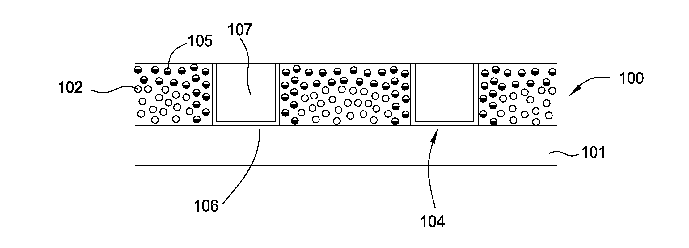
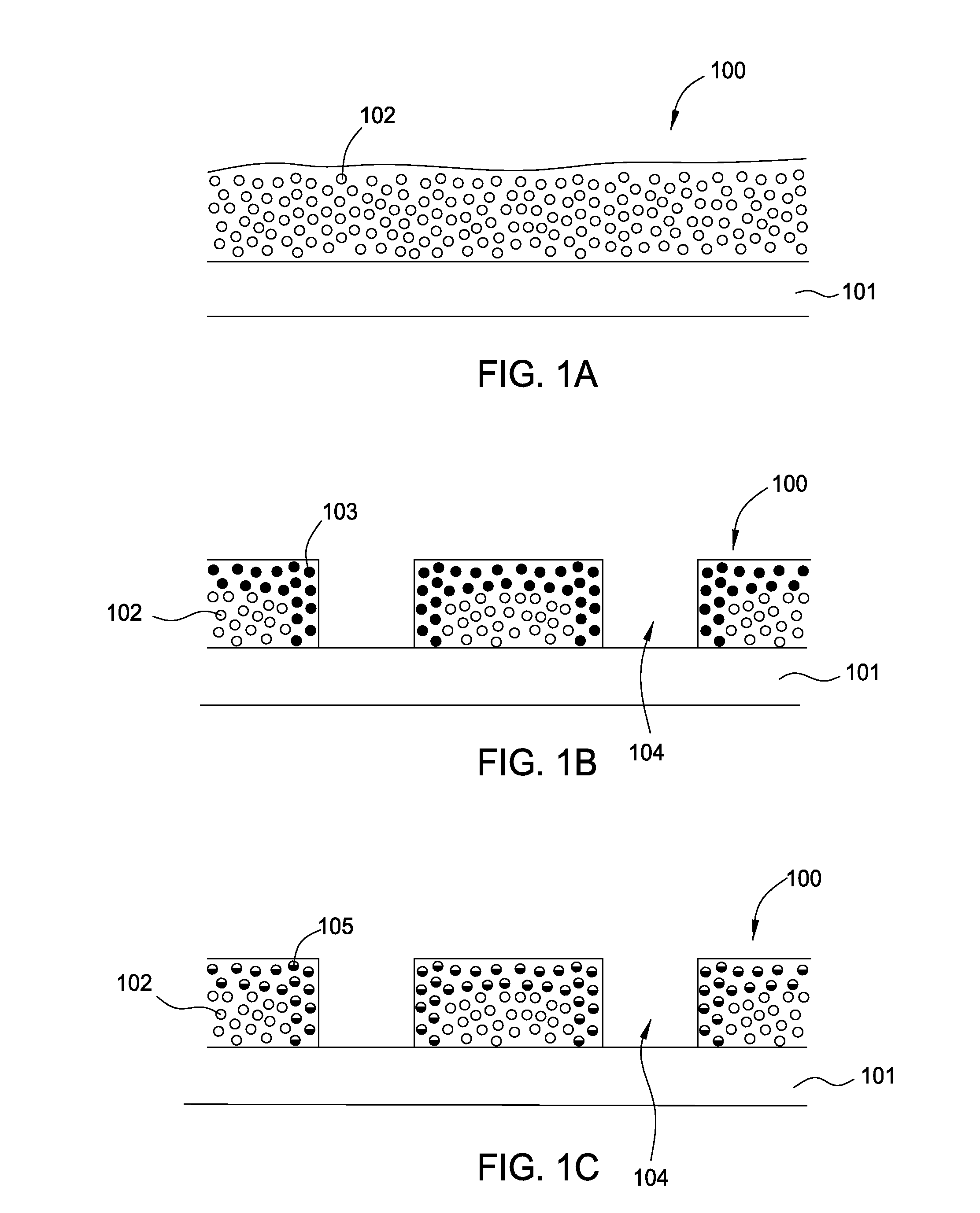
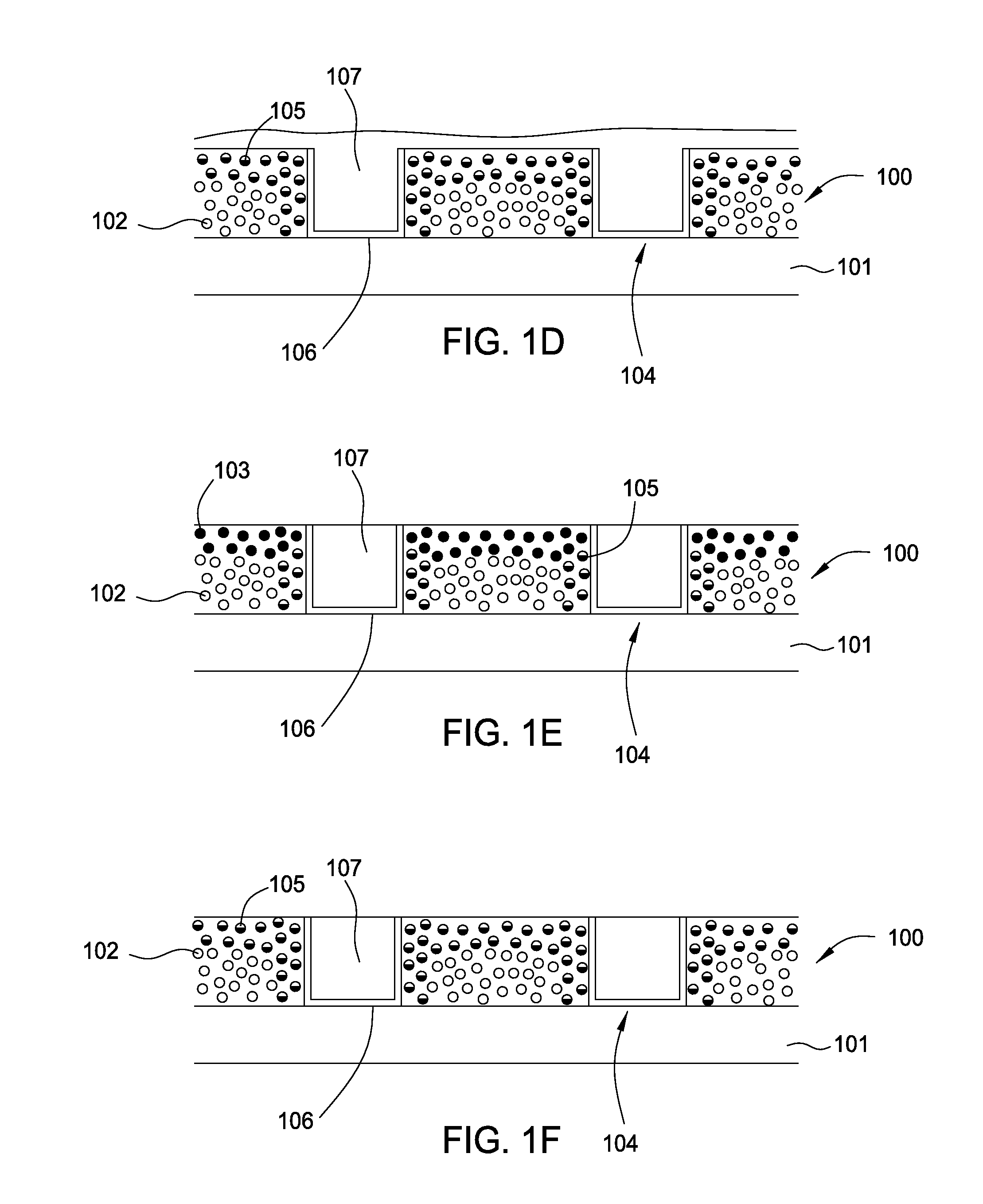
[0074]Direct Si—H Reduction via Chemical Exposure: a substrate containing a damaged porous CDO film is first placed inside a chamber. The chamber is then evacuated with the use of a vacuum pump. Following evacuation, trimethylvinylsilane (TMVS, CH2═CH—SiMe3) is introduced into the chamber. The Si—H moiety reacts with TMVS to form S1—CH2—CH2—SiMe3. An inert gas can be introduced at the same time. The process pressure can be at or lower than atmospheric pressure. The substrate temperature can be at room temperature or higher. Ultraviolet (UV) light exposure can be employed to assist / accelerate the reaction. The substrate is eventually removed from the chamber after exposure, possessing fewer Si—H bonds than it was before entering the chamber. Olefins, vinylsilanes, acetyl acetone, vinyl acetate, styrene, and acrylamide are known to react with Si—H, Chemicals in these families and derivatives thereof can be used in lieu of TMVS.

example 2

[0075]Indirect Si—H Reduction via Oxidation and Silylation: A substrate containing a damaged porous CDO film is first placed inside a chamber. The chamber is then evacuated with the use of a vacuum pump. Following evacuation, oxygen, nitrous oxide, ozone, or a mixture thereof is introduced into the chamber to effect oxidation of Si—H to form Si—OH. An inert gas can be introduced at the same time. The process pressure can be at or lower than atmospheric pressure. The substrate temperature can be at room temperature or higher. Ultraviolet (UV) light exposure can be employed to assist / accelerate the reaction. After oxidation, the substrate possesses fewer Si—H bonds and more Si—OH bonds than it did before entering the chamber. Silylation, a second step, is to follow oxidation. In this step, CTMS is introduced into the chamber to react with Si—OH to form Si—O—SiMe3. An inert gas can be introduced at the same time. The process pressure can be at or lower than atmospheric pressure. The su...

example 3

[0076]Simultaneous Si—H and Si—OH Reduction—Technique I: Si—H and Si—OH can be reduced at the same time. A substrate containing a damaged porous CDO film is first placed inside a chamber. The chamber is then evacuated with the use of a vacuum pump. Following evacuation, a mixture of TMVS and CTMS, one possible combination as an example, is introduced into the chamber to reduce both Si—H and Si—OH simultaneously. An inert gas can be introduced at the same time. The process pressure can be at or lower than atmospheric pressure. The substrate temperature can be at room temperature or higher. Ultraviolet (UV) light exposure can be employed to assist / accelerate the reaction. The substrate is eventually removed from the chamber after exposure, possessing fewer Si—H bonds and fewer Si—OH bonds than it was before entering the chamber.


PUM

PropertyMeasurementUnit
Temperatureaaaaaaaaaa
Pressureaaaaaaaaaa

Abstract

A method for repairing and lowering the dielectric constant of low-k dielectric layers used in semiconductor fabrication is provided. In one implementation, a method of repairing a damaged low-k dielectric layer comprising exposing the porous low-k dielectric layer to a vinyl silane containing compound and optionally exposing the porous low-k dielectric layer to an ultraviolet (UV) cure process.

Description

CROSS-REFERENCE TO RELATED APPLICATIONS[0001]This application claims benefit of U.S. provisional patent application Ser. No. 61 / 667,237, filed Jul. 2, 2012 which is herein incorporated by reference in its entirety.BACKGROUND[0002]1. Field[0003]Implementations of the present invention generally relate to repairing and lowering the dielectric constant of low-k dielectric films used in semiconductor fabrication.[0004]2. Description of the Related Art[0005]The dielectric constant (k) of dielectric films in semiconductor fabrication is continually decreasing as device scaling continues. Minimizing integration damage on low dielectric constant (low-k) films is important to be able to continue decreasing feature sizes. However, as feature sizes shrink, improvement in the resistive capacitance and reliability of dielectric films becomes a serious challenge.[0006]Porous low-k dielectric films including for example, carbon-doped oxides (CDO), experience damage to their bonding structures when...

Claims


Application Information

Patent Timeline
IPC IPC(8): H01L21/263
CPCH01L21/2636C23C16/045C23C16/401H01L21/02126H01L21/02203H01L21/02337H01L21/02348H01L21/3105H01L21/76814H01L21/76825H01L21/76826
Inventor CHAN, KELVINDEMOS, ALEXANDROS T.
Owner APPLIED MATERIALS INC
Learn More