Optoelectronic Semiconductor Chip and a Method for the Production Thereof

a technology of optoelectronic semiconductors and semiconductor chips, which is applied in the manufacture of semiconductor/solid-state devices, semiconductor devices, electrical appliances, etc., can solve the problems of exacerbated adverse effects of defects, leakage currents, and defects that diffuse into the semiconductor layer from the outside, so as to achieve advantageous output. , the effect of stable outpu

Inactive Publication Date: 2014-01-16
OSRAM OLED
View PDF3 Cites 1 Cited by
  • Summary
  • Abstract
  • Description
  • Claims
  • Application Information

AI Technical Summary

Benefits of technology

This patent describes how a mirror in a semiconductor chip can increase its reflectivity during operation, which helps to compensate for any ageing effects that occur over the lifetime of the chip. This results in a stable output from the chip and ensures a long-term, reliable performance. The change in reflectivity is achieved by the diffusion of silver out of one region of the chip into another, where it increases the reflectivity of the mirror during operation.

Problems solved by technology

In addition, defects may occur that diffuse into the semiconductor layers from the outside, for example, as a result of strains in other layers and assembly-related effects.
Such defects result inter alia in absorption of light, in a leakage current or in a change in or distortion of the lattice structure.
This adverse action of the defects is exacerbated by high currents during operation of the semiconductor chips, a high operating temperature, a high photon density, and the like.
For example, as a result of such action the output over the lifetime of the semiconductor chips is reduced, with the result that disadvantageous ageing effects occur over the lifetime of the semiconductor chips.

Method used


Image

  • Optoelectronic Semiconductor Chip and a Method for the Production Thereof
  • Optoelectronic Semiconductor Chip and a Method for the Production Thereof

Examples


Embodiment Construction

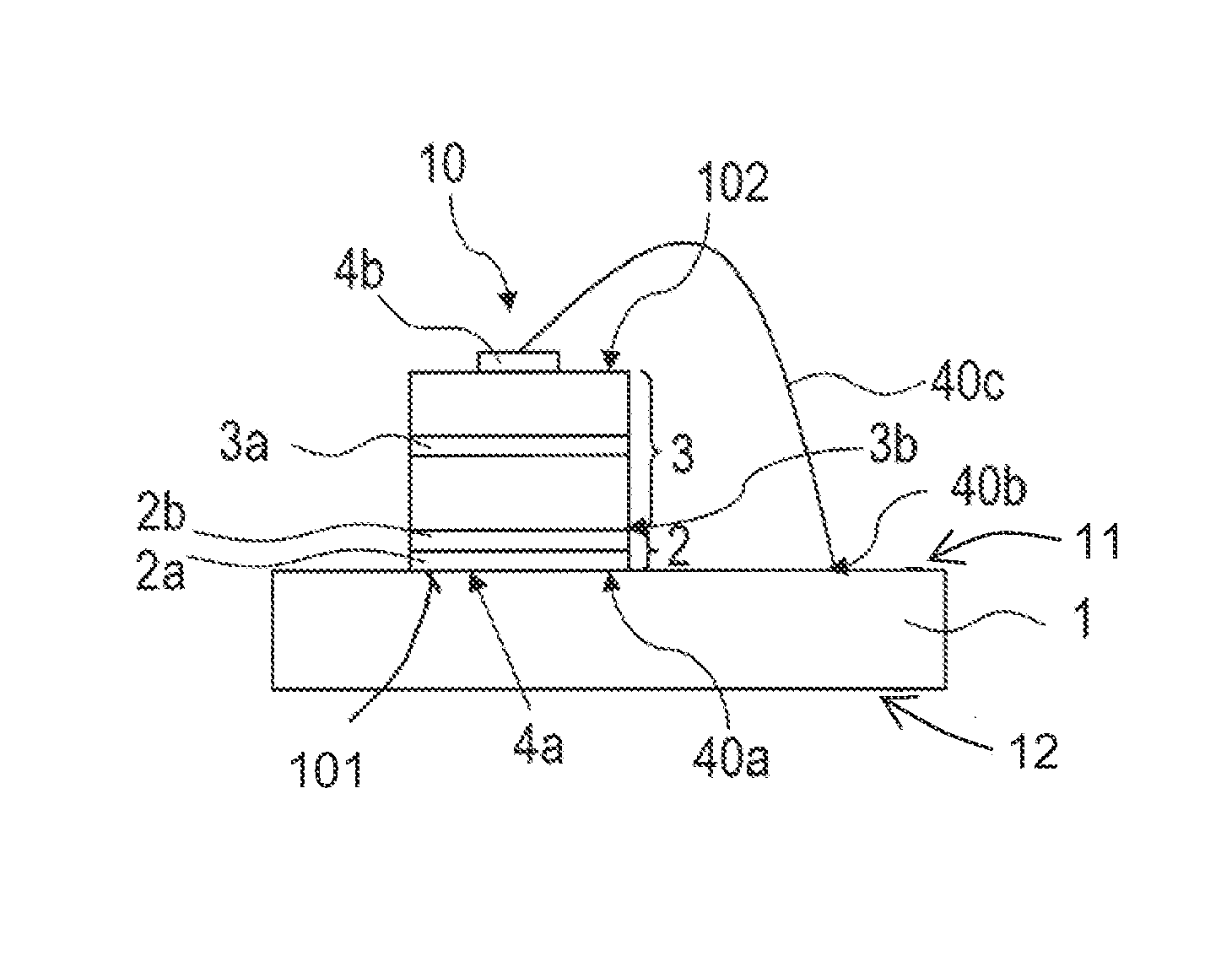
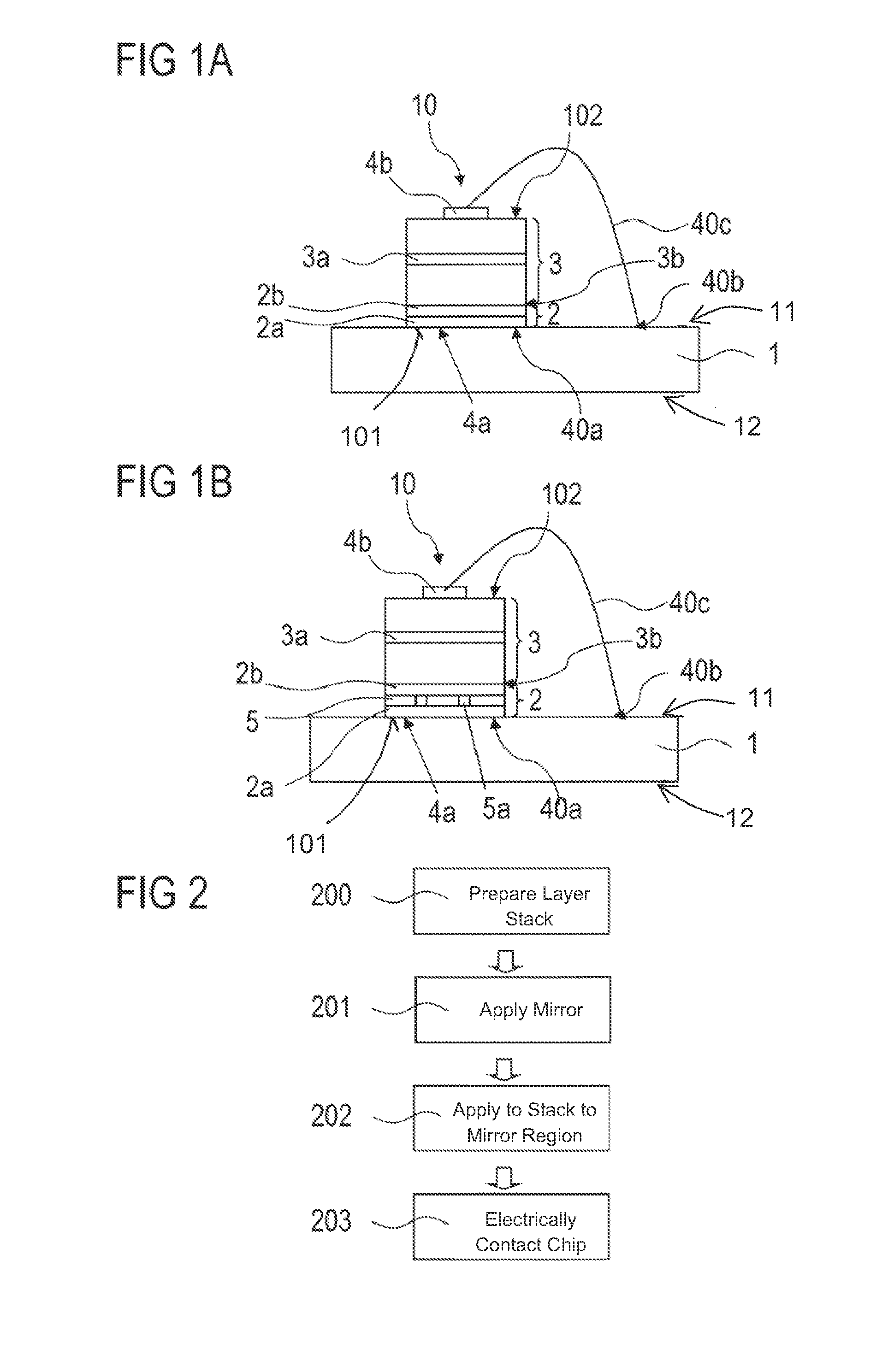
[0063]FIG. 1 shows a semiconductor chip 10 which is arranged on a printed circuit board 1. A carrier (not shown) can be arranged between the semiconductor chip 10 and the printed circuit board. The semiconductor chip 10 is an optoelectronic semiconductor chip, especially a radiation-emitting semiconductor chip. In particular, the semiconductor chip 10 is a thin-film LED.

[0064]The printed circuit board 1 has an upper side 1 and an underside 12. On the upper side 1 there is arranged a semiconductor layer stack 3 of the semiconductor chip 10. The printed circuit board with the semiconductor chip 10 mounted thereon can be attached externally (not shown) by its underside 12.

[0065]On the upper side 1 there are arranged electrically conductive conductor tracks 40a, 40b. The electrical conductor tracks 40a, 40b are arranged so as to be electrically insulated from one another. For example, the electrical insulation is effected by means of their being spaced apart or by means of an electrical...


PUM


Abstract

An optoelectronic semiconductor chip includes a semiconductor layer stack and a mirror. The semiconductor layer stack has an active layer for generating electromagnetic radiation. The mirror is arranged on an underside of the semiconductor layer stack. The mirror has a first region and a second region, the first region containing silver and the second region containing gold. A method of producing such a semiconductor chip is also defined.

Description

[0001]This patent application is a national phase filing under section 371 of PCT / EP2011 / 065950, filed Sep. 14, 2011, which claims the priority of German patent application 10 2010 046 089.3, filed Sep. 20, 2010, each of which is incorporated herein by reference in its entirety.TECHNICAL FIELD[0002]The present invention relates to an optoelectronic semiconductor chip and a method for the production thereof.BACKGROUND[0003]U.S. Patent Publication No. 2010 / 0032699 A1 defines a light-emitting diode.[0004]In conventional optoelectronic semiconductor chips, such as, for example, light-emitting diodes (LED), the output emitted by the component changes over its lifetime. For example, LEDs that emit radiation in the red wavelength range typically lose from 5 to 10% of their brightness during the first ten thousand hours of operation.[0005]The term “lifetime” is used in particular to define the period during which the brightness of the emitted radiation of the semiconductor chip falls to a d...

Claims


Application Information

Patent Timeline
Patent Type & Authority Applications(United States)
IPC IPC(8): H01L33/40
CPCH01L33/405H01L33/38H01L2224/32225H01L2224/48091H01L2224/48227H01L2224/73265H01L2924/01068
Inventor BEHRINGER, MARTIN RUDOLFKLEMP, CHRISTOPHRUPPRICH, CHRISTOPH
Owner OSRAM OLED
Why Eureka
Try Eureka