Self-aligned via interconnect using relaxed patterning exposure

a technology of self-alignment and patterning, applied in the direction of instruments, computer aided design, basic electric elements, etc., can solve the problems of limiting the achievable line-pattern density, the most lithographically challenging and costly steps in the integrated circuit manufacturing process, and the processing steps are among the most difficult and costly steps in the manufacturing process. achieve the effect of reducing the requirements for alignmen

Active Publication Date: 2014-01-16
SYNOPSYS INC
View PDF1 Cites 25 Cited by
  • Summary
  • Abstract
  • Description
  • Claims
  • Application Information

AI Technical Summary

Benefits of technology

[0004]Therefore, what is needed are systems and methods for self-aligned via interconnects using relaxed patterning exposure. What is additionally needed are systems and methods for self-aligned via interconnects using relaxed patterning exposure reduce the requirements for alignment of a via pattern mask. A further need exists for systems and methods for self-aligned via interconnects using relaxed patterning exposure that are compatible and complementary with existing systems and methods of integrated circuit design, manufacturing and test. Embodiments of the present invention provide these advantages.

Problems solved by technology

Unfortunately, due to a variety of factors, including, e.g., small via size and high density of vias, and because of the requirement to align the via pattern to the interacting wire patterns, the via processing steps are among the most lithographically challenging and costly steps in an integrated circuit manufacturing process.
Thus, a via pattern may frequently limit an achievable line-pattern density of the metal layers they connect.

Method used


Image

  • Self-aligned via interconnect using relaxed patterning exposure
  • Self-aligned via interconnect using relaxed patterning exposure
  • Self-aligned via interconnect using relaxed patterning exposure

Examples


Embodiment Construction

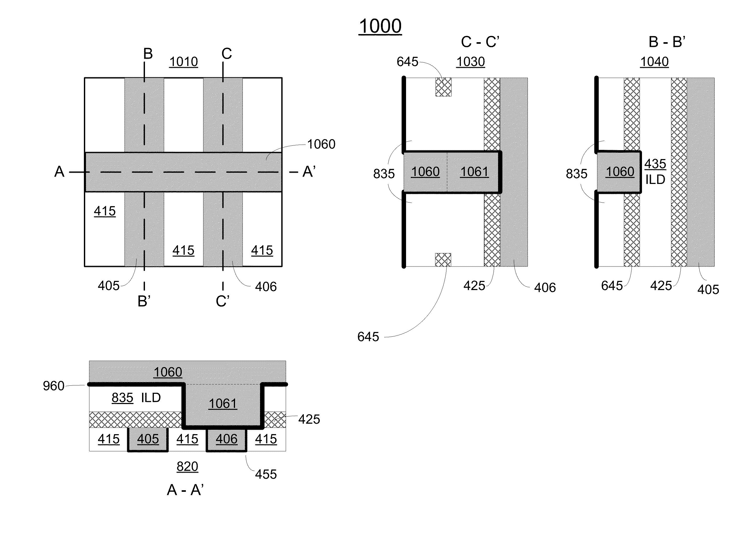
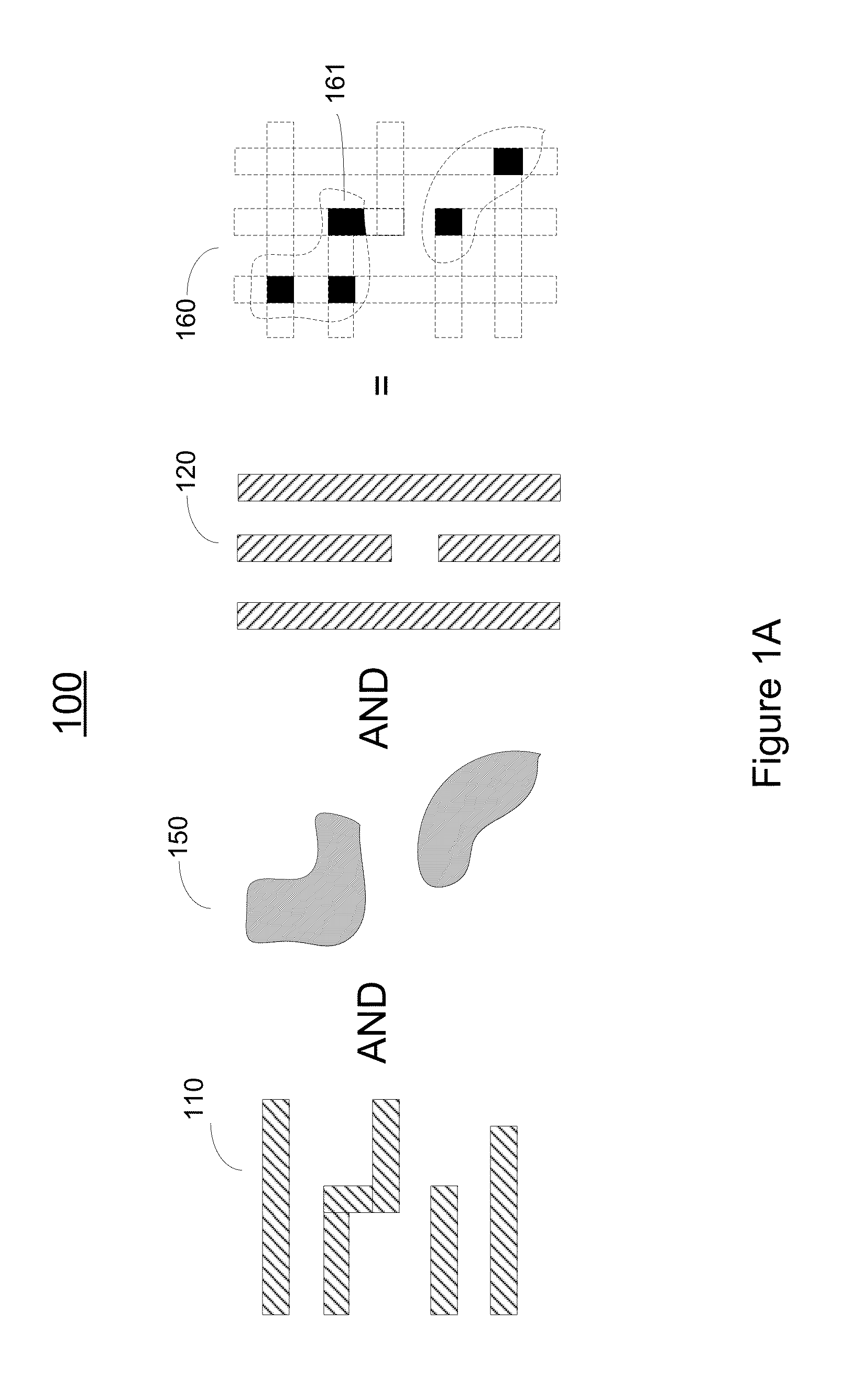
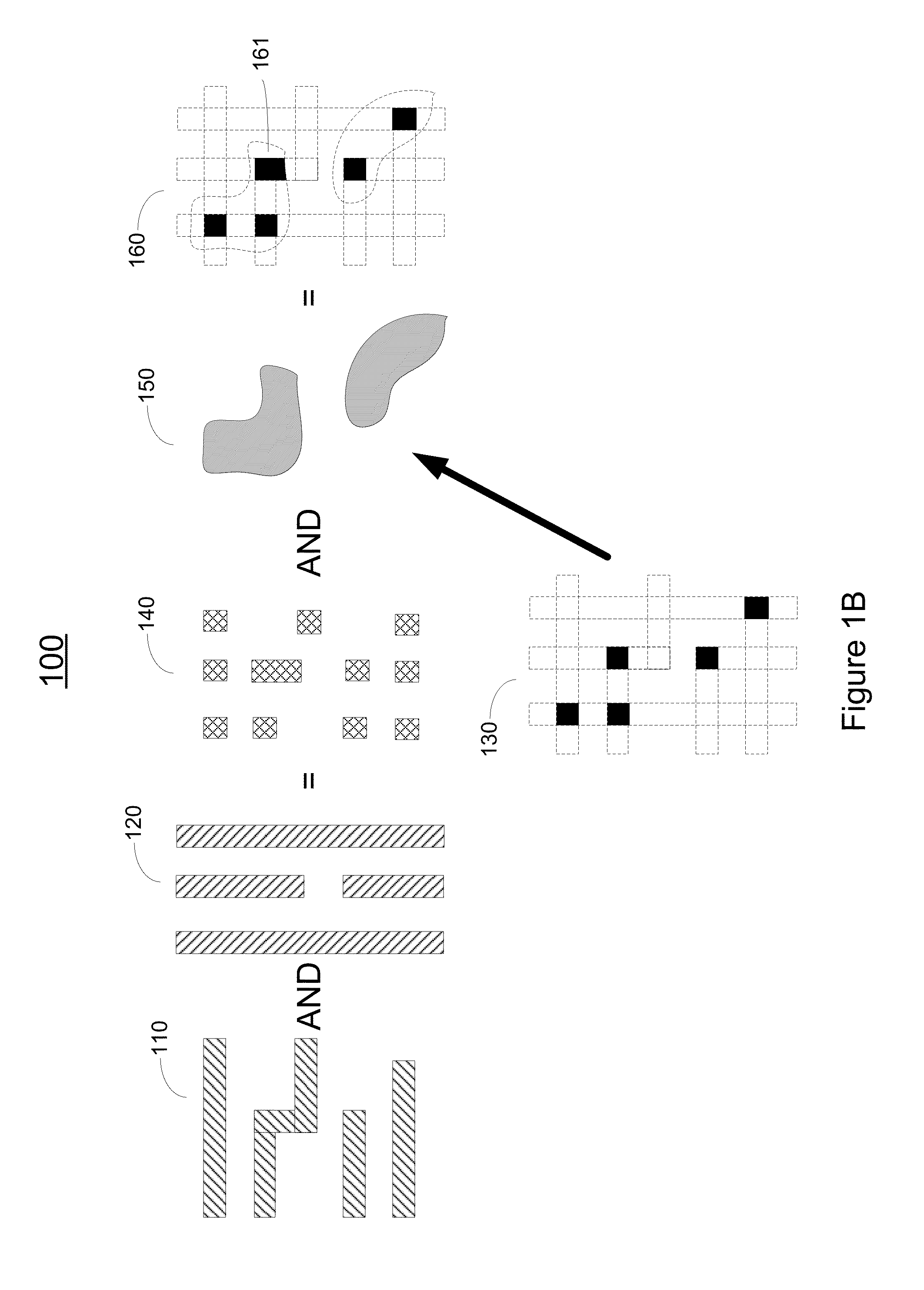
[0022]Reference will now be made in detail to various embodiments of the present invention, examples of which are illustrated in the accompanying drawings. While the invention will be described in conjunction with these embodiments, it is understood that they are not intended to limit the invention to these embodiments. On the contrary, the invention is intended to cover alternatives, modifications and equivalents, which may be included within the spirit and scope of the invention as defined by the appended claims. Furthermore, in the following detailed description of the invention, numerous specific details are set forth in order to provide a thorough understanding of the invention. However, it will be recognized by one of ordinary skill in the art that the invention may be practiced without these specific details. In other instances, well known methods, procedures, components, and circuits have not been described in detail as not to unnecessarily obscure aspects of the invention.

N...


PUM


Abstract

Self-aligned via interconnects using relaxed patterning exposure. In accordance with a first method embodiment, a method for controlling a computer-aided design (CAD) system for designing physical features of an integrated circuit includes accessing a first pattern for first metal traces on a first metal layer, accessing a second pattern for second metal traces on a second metal layer, vertically adjacent to the first metal layer and accessing a precise pattern of intended interconnections between the first and second metal traces. The precise pattern of intended interconnections is operated on to form an imprecise via pattern that indicates a plurality of general areas in which vias are allowed. The imprecise via pattern is for use in an integrated circuit manufacturing process to form, in conjunction with operations to form the first and second metal layers, a plurality of self-aligned vias for interconnecting the intended interconnections.

Description

FIELD OF INVENTION[0001]Embodiments of the present invention relate to the field of integrated circuit design and manufacture. More specifically, embodiments of the present invention relate to systems and methods for self-aligned via interconnects using relaxed patterning exposure.BACKGROUND[0002]In integrated circuits, traces or “wires” on various layers are electrically connected to traces on other layers by means of vertical metal “vias” between such layers. Under the conventional art, the pattern of vias between two layers, e.g., wiring or metal layers, is completely defined lithographically by exposing an image of a mask via pattern, etching holes in the separating dielectric, and then filling the holes with metal, e.g., copper.[0003]Unfortunately, due to a variety of factors, including, e.g., small via size and high density of vias, and because of the requirement to align the via pattern to the interacting wire patterns, the via processing steps are among the most lithographic...

Claims


Application Information

Patent Timeline
Patent Type & Authority Applications(United States)
IPC IPC(8): H01L21/768H01L23/538G06F17/50
CPCH01L21/76877G06F17/5072H01L23/5384G06F30/392H01L23/5226H01L23/53295H01L21/76816H01L21/76897H01L2924/0002H01L2924/00H01L23/53228
Inventor RIEGER, MICHAEL L.MOROZ, VICTOR
Owner SYNOPSYS INC
Why Eureka
Try Eureka