Semiconductor device, method for manufacturing same and thin plate interconnect line member

Active Publication Date: 2007-11-27
SEMICON COMPONENTS IND LLC
View PDF22 Cites 21 Cited by
  • Summary
  • Abstract
  • Description
  • Claims
  • Application Information

AI Technical Summary

Benefits of technology

[0027]The method according to the present invention may also include the configuration, in which the base is an electrical conductive base, and at least a part of the metal film is formed via an electrolytic plating method, in which the electrical conductive base is utilized as an electrode thereof. Having this configuration, the metal film can be formed to a desired thickness with improved process controlla

Problems solved by technology

However, it is still difficult to achieve the levels of miniaturization, the reduction of the thickness and the reduction of the weight of the package that are currently desired in the market of the portable electronics products or the like, by employing the conventional CSP.
The

Method used


Image

  • Semiconductor device, method for manufacturing same and thin plate interconnect line member
  • Semiconductor device, method for manufacturing same and thin plate interconnect line member
  • Semiconductor device, method for manufacturing same and thin plate interconnect line member

Examples


example 1

[0090]The high frequency performance of the insulating resin used for the semiconductor device was evaluated in the first example. Samples for the evaluation were manufactured by disposing an underlying line, disposing an interlayer insulating film thereon, disposing an upper line thereon, and providing an interlayer coupling plug that couples the underlying line to the upper line to form a structure. Two types of samples were prepared: one comprises a sealant resin layer disposed directly thereon without intervening a solder resist layer; and the other comprises a sealant resin layer disposed on the surface of the upper line via a solder resist layer. The interconnect lines were formed of copper-plated film, and the dimension thereof for both the underlying layer and the upper layer was: a width of 90 μm and a length of 10 mm. The surface roughness Ra of the copper film was 0.8 μm.

[0091]The following sample 1 and sample 2 comprising different resin materials for the interlayer insu...

example 2

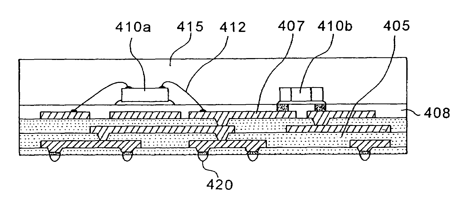
[0095]Semiconductor devices having dual interconnect line structure were manufactured in a similar process as shown in FIGS. 5A, 5B, 5C, 6A, 6B and 7. LSI chips, CR chips, TR chips or the like were disposed on the upper surface of the interconnect line structure. Copper was employed for the material of the interconnect line. The surface roughness Ra of the copper film formed by the same process as employed in this example was 0.8 μm. The materials used for the interlayer insulating film were shown in Table-1, and the three types of samples (sample NO. 1 to 3) were prepared.

[0096]

TABLE 1No.123resin typeliquidepoxy resinBT resincrystalpolymerdielectric 2.853.6, 3.7 3.4constant(1 GHz)(1 MHz)(1 GHz)dielectric 0.00250.003, 0.006 0.003loss(1 GHz)(1 MHz)(1 GHz)tangentglass205230220transitiontemperaturecopper foil 0.91.4 1.5peelingtest (18 or 35 μm)kN / mwater 0.04 0.1absorption (%)manufacturerKURARAYSUMITOMOMITSUBISHIBAKELITEGAS CHEMICALproductVecstarELC-4778GSHL950K-SKname

[0097]The intercon...

example 3

[0098]The high frequency performance of the insulating resin used for the semiconductor device, in which wholly aromatic polyester liquid crystal polymers described below having different coefficient of thermal expansion are used as the interlayer insulating film insulating, was evaluated in this example. Samples for the evaluation were manufactured by disposing an underlying line, disposing an interlayer insulating film thereon, disposing an upper line thereon, and providing an interlayer coupling plug that couples the underlying line to the upper line to form a structure.

[0099]Sample 3: wholly aromatic polyester liquid crystal polymer, commercially available under the trade name of “Vecstar FA” by KURARAY, Osaka Japan, coefficient of thermal expansion: −5 (ppm / degree centigrade);

[0100]Sample 4: wholly aromatic polyester liquid crystal polymer, commercially available under the trade name of “Vecstar OC” by KURARAY, Osaka Japan, coefficient of thermal expansion: 5 (ppm / degree centig...


PUM

PropertyMeasurementUnit
Lengthaaaaaaaaaa
Water absorptionaaaaaaaaaa
Structureaaaaaaaaaa

Abstract

The present invention provides a low-profile and light-weight semiconductor device having improved product reliability and higher frequency performance. A multi-layer interconnect line structure is disposed just under circuit devices 410a and 410b. An Interlayer insulating film 405 that composes a part of the multi-layer interconnect line structure is formed of a material having a relative dielectric constant within a range from 1.0 to 3.7, and a dielectric loss tangent within a range from 0.0001 to 0.02.

Description

[0001]This application is based on Japanese patent application NO.2002-351827, the content of which is incorporated hereinto by reference.BACKGROUND OF THE INVENTION[0002]1. Field of the Invention[0003]The present invention relates to a semiconductor device, which mounts semiconductor chips or the like thereon, and is coupled to interconnect line substrates or the like, and a method for manufacturing same, and also relates to a thin plate interconnect line member employed for the semiconductor device.[0004]2. Description of the Related Art[0005]Portable electronics products such as cellular phone, PDA, DVC, DSC or the like acquire multi-functions in an accelerating speed, and in such condition the miniaturization and the weight reduction is essential for these products to be accepted by the market, and thus LSI having higher integration level are necessary to satisfy these needs. On the other hand, more user-friendly and convenient products are also desired for these electronics pro...

Claims


Application Information

Patent Timeline
IPC IPC(8): H01L23/04H01L23/498H05K1/00H05K1/02H05K3/20H05K3/46
CPCH01L21/6835H01L23/49822H01L23/49838H01L23/49894H01L24/97H05K3/4682H01L2221/68345H01L2224/48091H01L2224/49171H01L2224/73265H01L2224/97H01L2924/01005H01L2924/01013H01L2924/01015H01L2924/0102H01L2924/01027H01L2924/01029H01L2924/01033H01L2924/01046H01L2924/01047H01L2924/01078H01L2924/01079H01L2924/01082H01L2924/01088H01L2924/14H01L2924/15311H01L2924/19041H01L2924/19043H01L2924/19105H01L2924/30105H05K1/024H05K3/205H05K3/4676H05K2201/068H01L24/48H01L24/49H01L2924/01006H01L2924/01019H01L2924/01023H01L2924/01024H01L2924/01087H01L2224/16225H01L2224/32225H01L2224/73204H01L2224/45144Y10S428/901H01L2924/13055H01L24/45Y10T428/24917H01L2224/85H01L2924/00014H01L2224/81H01L2224/83H01L2924/00H01L2924/12042H01L2924/181H01L2924/00012H01L2224/0401
Inventor USUI, RYOSUKEMIZUHARA, HIDEKIIGARASHI, YUSUKEKOJIMA, NORIAKISAKAMOTO, NORIAKI
Owner SEMICON COMPONENTS IND LLC
Why Eureka
Try Eureka