Liquid crystal display device

a liquid crystal display and liquid crystal technology, applied in static indicating devices, non-linear optics, instruments, etc., can solve the problems of discoloration of the liquid crystal layer, the local temperature elevation of the liquid crystal in the vicinity of the driver, and etc., to suppress the transmission of stress, enhance numerical aperture, and suppress the displacement of alignment

Inactive Publication Date: 2007-01-16
PANASONIC LIQUID CRYSTAL DISPLAY CO LTD +1
View PDF6 Cites 20 Cited by
  • Summary
  • Abstract
  • Description
  • Claims
  • Application Information

AI Technical Summary

Benefits of technology

[0030]Accordingly, it is an object of the present invention to provide a liquid crystal display device which can solve the drawback which is explained in conjunction with the above-mentioned first problem, that is, which can suppress the local temperature elevation of a liquid crystal in the vicinity of drivers.
[0031]It is another object of the present invention to provide a liquid crystal display device which can solve the drawback which is explained in conjunction with the above-mentioned second problem, that is, which can suppress the transmission of the stress from drivers to the substrate.
[0032]It is still another object of the present invention to provide a liquid crystal display device which can solve the drawback which is explained in conjunction with the abovementioned third problem, that is, which can suppress the alignment displacement on the display surface in the vicinity of the drivers.
[0033]It is a further object of the present invention to provide a liquid crystal display device which can solve the drawback which is explained in conjunction with the above-mentioned fourth problem, that is, which can enhance the numerical aperture.
[0034]It is a still further object of the present invention to provide a liquid crystal display device which can solve the drawback which is explained in conjunction with the abovementioned fifth problem, that is, which can achieve a so-called shrinkage of the picture frame.

Problems solved by technology

However, the lateral electric field method adopts a birefringence refraction mode as a display mode of a liquid crystal thereof and hence, the mode is sensitive to the fluctuation of a thickness of a liquid crystal layer compared to the TN mode whereby there arises a drawback that the liquid crystal layer appears more colored with respect to the same fluctuation quantity of the thickness of the liquid crystal layer.
Further, inventors of the present invention have found out that, in the FCA method, the drivers are directly mounted on the substrate of the liquid crystal display device and hence, the generated heat from the drivers are directly transmitted to the substrate of the liquid crystal display device so that there arises a drawback that the liquid crystal in the vicinity of the drivers exhibits the local temperature elevation and this portion appears discolored.

Method used


Image

  • Liquid crystal display device
  • Liquid crystal display device
  • Liquid crystal display device

Examples


embodiment 1

(Embodiment 1)

(Equivalent Circuit of Liquid Crystal Display Device)

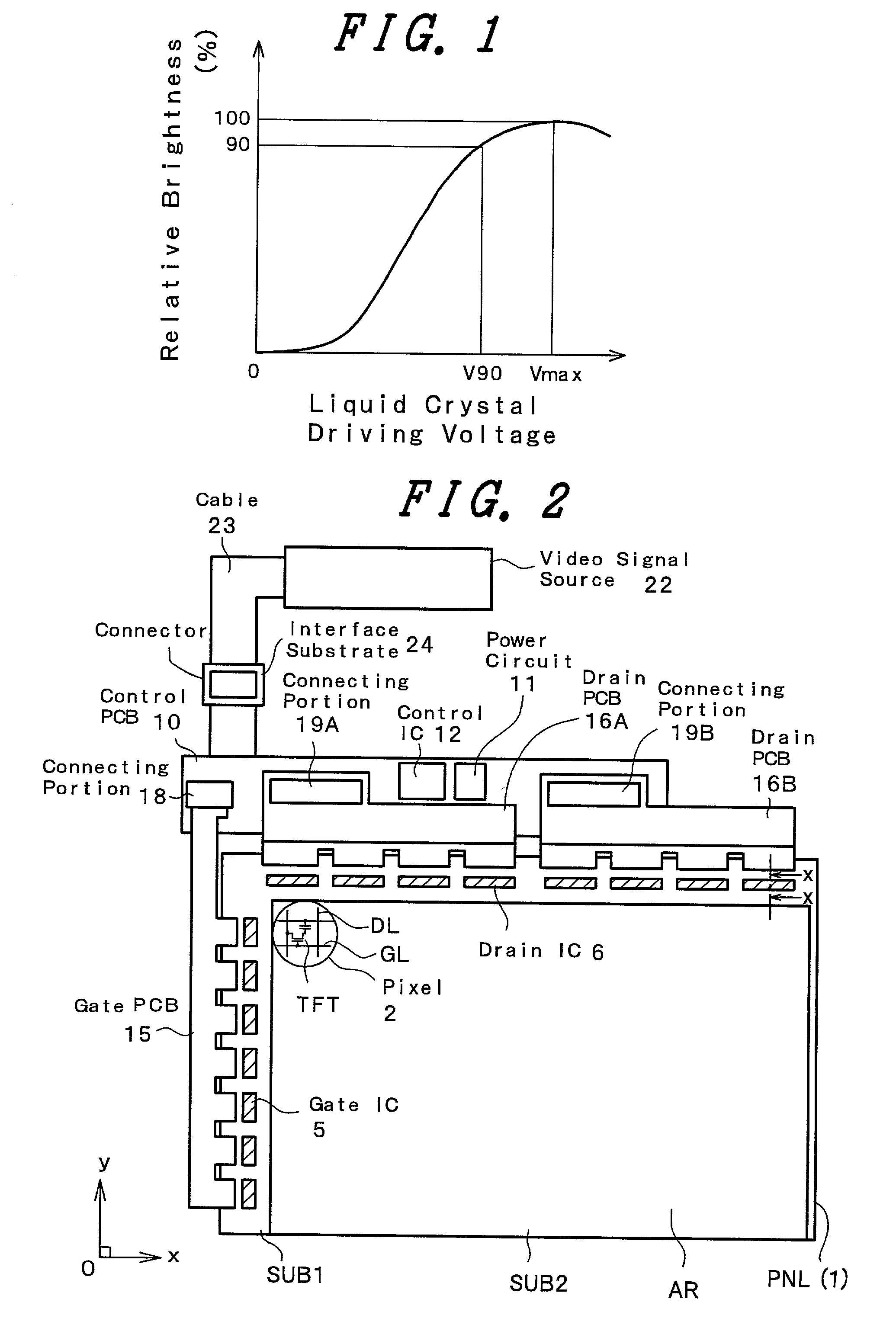
[0121]FIG. 2 is an equivalent circuit block diagram showing one embodiment of a liquid crystal display device according to the present invention. Although this drawing is a circuit block diagram, they are drawn corresponding to the actual geometric arrangement.

[0122]In this embodiment, the present invention is applied to a liquid crystal display device which adopts a so-called lateral electric field method which is known as a method having a broad viewing angle.

[0123]First, the liquid crystal display device includes a liquid crystal display panel PNL and this liquid crystal display panel PNL uses transparent substrates SUB1, SUB2 which are arranged to face each other in an opposed manner while sandwiching a liquid crystal between them as an envelope. In this case, one transparent substrate (in the drawing, a lower-side substrate: a matrix substrate) is formed slightly larger than the other transparent substrate (in t...

embodiment 2

(Embodiment 2)

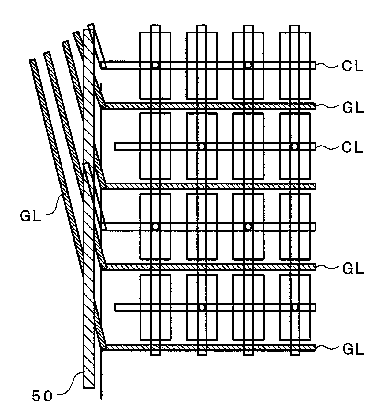
[0167]This embodiment is characterized in that reference signals which are supplied to the reference electrodes CT of each pixel region via the reference voltage signal line CL are inverted every frame.

[0168]As shown in FIG. 7, this implies that the amplitude V of the video signals is determined in response to the reference signals which are inverted by a unit of a frame and hence, the amplitude of the video signals can be made small as a whole.

[0169]Ton consider a case in which the reference signals are set constant by a unit of a frame as shown in FIG. 8 for a comparison purpose, it is necessary for the video signals to take an amplitude V in the (+) side and an amplitude V in the (−) side in response to the reference signals.

[0170]Accordingly, this embodiment can reduce the amplitude of the video signal by half compared to FIG. 8.

[0171]This implies that as the drain drive IC, a drain drive IC with a small output can be selected and a heat generation quantity can be ...

embodiment 3

(Embodiment 3)

[0172]In this embodiment, out of the drain signal line DL and the reference voltage signal line CL, the signal line to which signals having a larger average voltage amplitude by a unit of a frame are supplied is set to have a resistance lower than that of the other signal line.

[0173]Although various drive waveforms which are inputted to the signal lines exhibit a shape approximating a rectangular shape as shown in FIG. 9(a) at an input end thereof, they exhibit a deformed waveform as shown in FIG. 9(b) at a remote end thereof due to the resistance of the signal lines or the parasitic capacity.

[0174]A uniform display is required on the entire region of the display surface of the liquid crystal display panel PNL and hence, it is necessary for the actual input signals to preliminarily increase the amplitude of the input voltage in consideration of a distortion amount of this waveform. However, the driving voltage is required to be elevated further correspondingly.

[0175]Ac...


PUM

PropertyMeasurementUnit
relative transmittivityaaaaaaaaaa
transmittivityaaaaaaaaaa
thicknessaaaaaaaaaa

Abstract

A liquid crystal display device can suppress the local temperature elevation of a liquid crystal in the vicinity of drivers. On a liquid-crystal-side surface of one substrate out of substrates which are arranged to face each other in an opposed manner while sandwiching a liquid crystal therebetween, a switching element which is operated in response to scanning signals from a gate signal line, a pixel electrode to which video signals from a drain signal line are supplied via the switching element, and a reference electrode which generates an electric field between the reference electrode and the pixel electrode are mounted on each pixel region of the liquid-crystal-side surface. The video signals from the drain signal line are generated by a driver chip mounted on one substrate. A light transmittivity of the liquid crystal layer is set to take a minimum value when a voltage is not applied between the pixel electrode and the reference electrode. A maximum amplitude of voltage of the video signals is set to a value not more than a voltage necessary for setting a relative transmittivity of the liquid crystal layer to 90%.

Description

BACKGROUND OF THE INVENTION[0001](1) Field of the Invention[0002]The present invention relates to a liquid crystal display device, and more particularly, to an active-matrix type liquid crystal display device.[0003](2) Background Art[0004]In an active-matrix type liquid crystal display device, on a liquid-crystal-side surface of one substrate out of respective substrates which are arranged to face each other in an opposed manner while sandwiching a liquid crystal therebetween, respective regions which are surrounded by gate signal lines which are extended in the x direction and are arranged in the y direction in parallel and drain signal lines which are extended in the y direction and are arranged in the x direction in parallel are formed as pixel regions. Each pixel region includes an active element which is operated in response to scanning signals from the gate signal line, a pixel electrode to which video signals from the drain signal line are supplied via the active element, and...

Claims


Application Information

Patent Timeline
Patent Type & Authority Patents(United States)
IPC IPC(8): G09G3/36G02F1/1337G02F1/13G02F1/133G02F1/1343G02F1/1345G02F1/1368
CPCG02F1/134363G09G3/3648G02F1/13452G02F1/1345G02F1/133
Inventor YANAGAWA, KAZUHIKOIWAKABE, YASUSHINAKAYOSHI, YOSHIAKIKOBAYASHI, SETSUOKONDO, KATSUMIKURAHASHI, NAGATOSHI
Owner PANASONIC LIQUID CRYSTAL DISPLAY CO LTD
Why Eureka
Try Eureka