Light emitting device and manufacturing method thereof
a technology of light-emitting devices and manufacturing methods, which is applied in the direction of cathode ray tubes/electron beam tubes, lamp details, electric discharge tubes, etc., can solve the problems of low luminescent efficiency and opaque ceramics, and achieve the effect of simple manufacturing process and low cos
- Summary
- Abstract
- Description
- Claims
- Application Information
AI Technical Summary
Benefits of technology
Problems solved by technology
Method used
Image
Examples
example 1
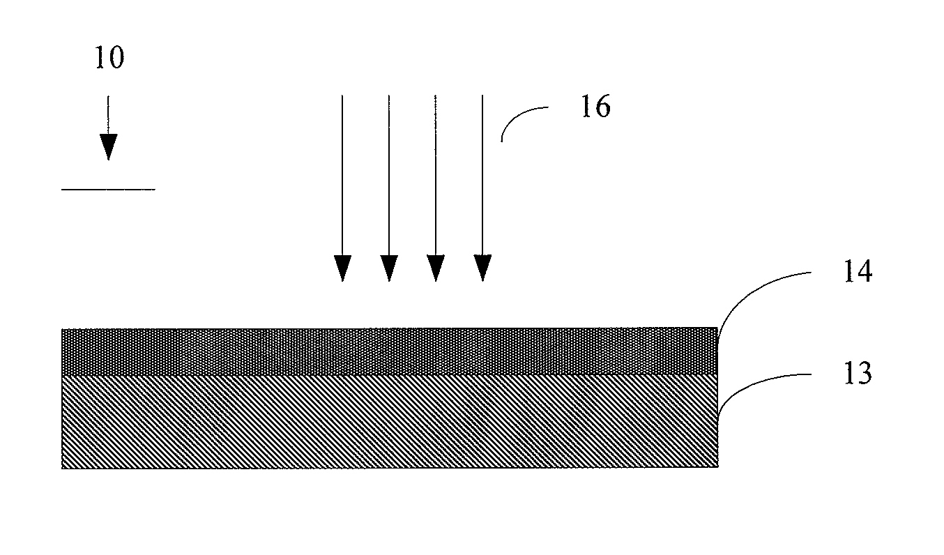
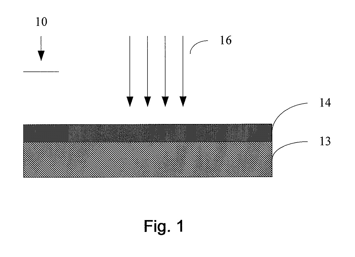
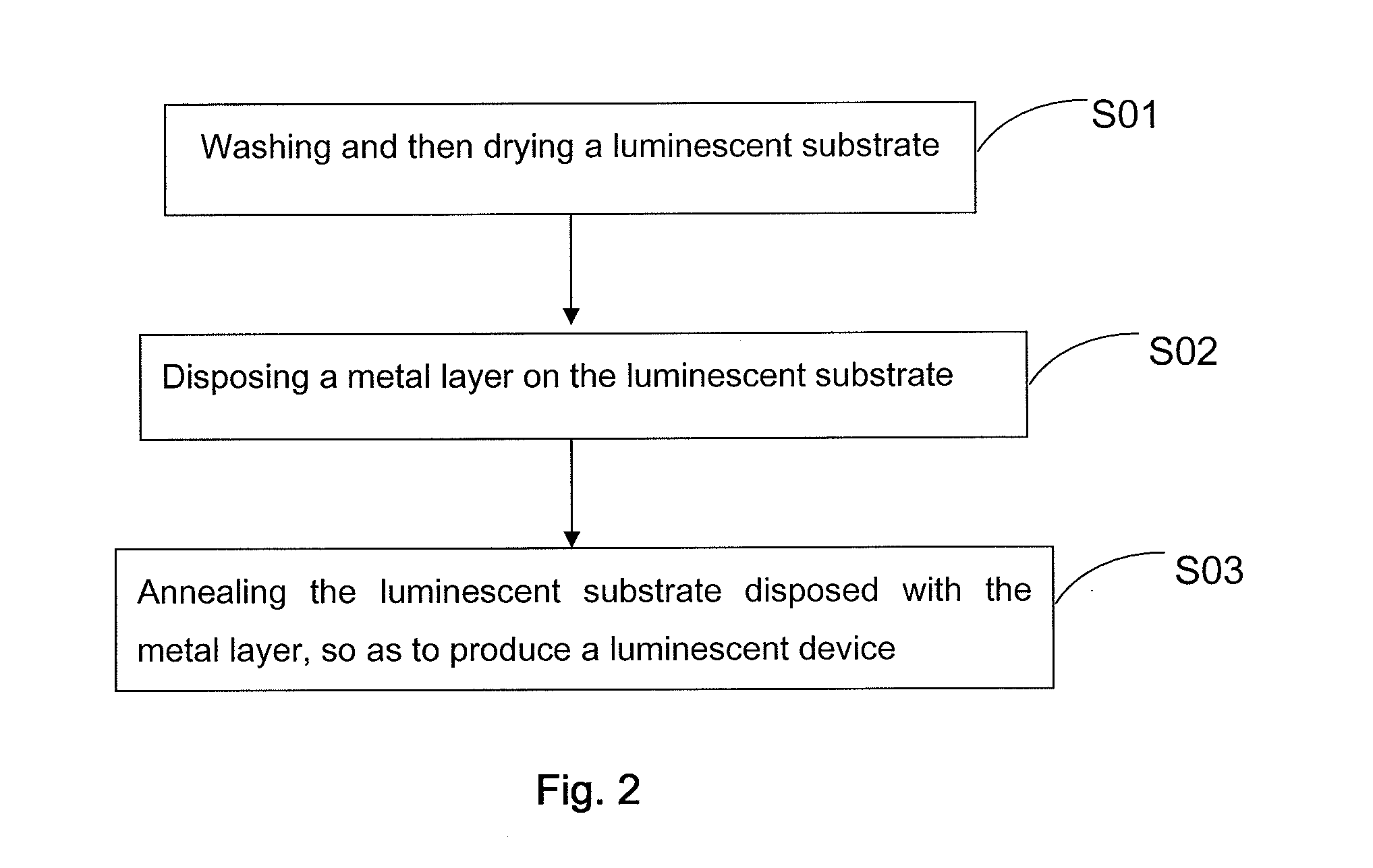
[0038]A Eu-doped Y2O3 series transparent ceramic plate, i.e. a luminescent ceramic having a formula of Y2O3:Eu, is used as the luminescent substrate. A silver layer having a thickness of 20 nm is deposited on a surface of the transparent ceramic plate with a megnetron sputtering equipment. The resulted device is placed in a vacuum environment have a vacuity of −3 Pa, annealed at 300° C. for half an hour, and then cooled to room temperature, to give a luminescent device with a metal layer having a metal microstructure.
[0039]A spectral test is carried out on the luminescent device manufactured above, wherein the luminescent device is bombarded by cathode rays produced by an electron gun. An electron beam first passes through the metal layer and then excites transparent ceramic Y2O3:Eu to emit light, yielding a luminescent spectrum as shown in FIG. 4. The spectrum in the figure shows that the luminescent material is a green-light-emitting luminescent material. Curve 11 in the figure re...
example 2
[0040]Example 2 is basically the same as Example 1, excepted that a gold layer having a thickness of 200 nm is deposited on a surface of the luminescent substrate, the resulted device is placed in a vacuum environment have a vacuity of −3 Pa, annealed at 650° C. for 1 hour, and then cooled to room temperature, to give a luminescent device with a metal layer having a metal microstructure.
example 3
[0041]Example 3 is basically the same as Example 1, excepted that an aluminum layer having a thickness of 0.5 nm is deposited on a surface of the luminescent substrate, the resulted device is placed in a vacuum environment have a vacuity of −3 Pa, annealed at 50° C. for 5 hours, and then cooled to room temperature, to give a luminescent device with a metal layer having a metal microstructure.
PUM
 Abstract
Description
Claims
Application Information
 - R&D
- Intellectual Property
- Life Sciences
- Materials
- Tech Scout
- Unparalleled Data Quality
- Higher Quality Content
- 60% Fewer Hallucinations
Browse by: Latest US Patents, China's latest patents, Technical Efficacy Thesaurus, Application Domain, Technology Topic, Popular Technical Reports.
© 2025 PatSnap. All rights reserved.Legal|Privacy policy|Modern Slavery Act Transparency Statement|Sitemap|About US| Contact US: help@patsnap.com


