Interface adhesion improvement method

a technology of interface adhesion and improvement method, which is applied in the direction of photovoltaic energy generation, coatings, chemical vapor deposition coatings, etc., can solve the problems of poor surface adhesion at the interface, increased the likelihood of film cracking, and device failur

Active Publication Date: 2014-01-23
APPLIED MATERIALS INC
View PDF12 Cites 45 Cited by
  • Summary
  • Abstract
  • Description
  • Claims
  • Application Information

AI Technical Summary

Problems solved by technology

However, different materials, especially organic and inorganic materials, often have different film properties, thereby resulting in poor surface adhesion at the interface where the organic and the inorganic layers are in contact with.
Poor interface adhesion often allows film peeling or particle generation, thereby adversely contaminating the device structure 100 and eventually leading to device failure.
Additionally, poor adhesion at the interface 114 may also increase the likelihood of film cracking, thereby allowing the moisture or air to sneak into the device structure 100, thereby deteriorating the device electrical performance.

Method used


Image

  • Interface adhesion improvement method
  • Interface adhesion improvement method
  • Interface adhesion improvement method

Examples


Embodiment Construction

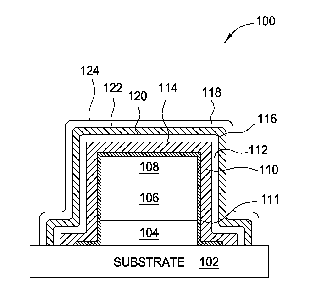
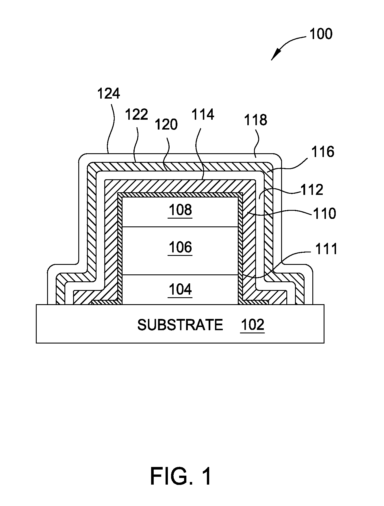
[0023]Embodiments of the present invention include methods for improving surface adhesion at an interface with different materials for improving surface adhesion for the encapsulating layers passivating a device structure. In some embodiments, the invention may be advantageously used in OLED applications or thin film transistor applications. In one embodiment, the interface adhesion is improved by forming a buffer layer between film layers of different materials or of different film properties. The buffer layer may be a silicon containing or nitrogen containing dielectric layer. In another embodiment, the interface adhesion is improved by performing a plasma treatment process at the interface between film layers of different materials or of different film properties. As the plasma treatment process alters at least some of surface properties, e.g., wetability or surface roughness, atoms from the subsequent deposited layer to be adhered more securely on the interface as compared to co...


PUM

PropertyMeasurementUnit
temperatureaaaaaaaaaa
refractive indexaaaaaaaaaa

Abstract

Embodiments of the invention provide methods of an interface adhesion improvement methods used on a transparent substrate for OLED or thin film transistor applications. In one embodiment, a method of forming a buffer layer on a surface of a substrate includes providing a substrate having an planarization material disposed thereon in a processing chamber, supplying a buffer layer gas mixture including a silicon containing gas into the processing chamber, controlling a substrate temperature less than about 100 degrees Celsius, forming a buffer layer on the planarization material, supplying an encapsulating barrier layer deposition gas mixture including a silicon containing gas and a nitrogen containing gas into the processing chamber, and forming an encapsulating barrier layer on the buffer layer.

Description

CROSS-REFERENCE TO RELATED APPLICATIONS[0001]This application claims benefit of U.S. Provisional Application Ser. No. 61 / 674,028 filed Jul. 20, 2012 (Attorney Docket No. APPM / 17628L), which is incorporated by reference in their entirety.BACKGROUND OF THE INVENTION[0002]1. Field of the Invention[0003]Embodiments of the present invention generally relate to methods for improving interface adhesion. More particularly, embodiments of the present invention relate to interface adhesion improvement methods performed on a surface of a substrate used in thin-film transistor or OLED applications.[0004]2. Description of the Related Art[0005]Organic light emitting diode (OLED) displays have gained significant interest recently in display applications in view of their faster response times, larger viewing angles, higher contrast, lighter weight, lower power and amenability to flexible substrates. Generally, a conventional OLED is enabled by using one or more layers of organic materials sandwiche...

Claims


Application Information

Patent Timeline
Patent Type & Authority Applications(United States)
IPC IPC(8): H01L21/02
CPCH01L21/02107C23C16/308Y02E10/549H10K77/10H10K59/873H10K50/844
Inventor CHOI, YOUNG JINCHEN, JRJYAN JERRYPARK, BEOM SOOCHOI, SOO YOUNG
Owner APPLIED MATERIALS INC
Why Eureka
Try Eureka