Atomic Layer Deposition with Plasma Source

a technology of atomic layer and plasma source, which is applied in the direction of plasma technique, chemical vapor deposition coating, coating, etc., can solve the problems of complex deposition cycle, specific problems, and certain requirements

Active Publication Date: 2014-01-23
PICOSUN OY
View PDF1 Cites 120 Cited by
  • Summary
  • Abstract
  • Description
  • Claims
  • Application Information

AI Technical Summary

Benefits of technology

[0025]In certain embodiments, the apparatus or control system is configured to allow gas from the inactive gas source to flow into the radical in-feed part via the plasma source during a purge period of a plasma atomic layer deposition period, the gas during that purge period functioning as purge and inert shield gas.
[0026]In certain embodiments, the apparatus or control system is configured to allow gas from the inactive gas source to flow into the radical in-feed part via the plasma source both during a plasma atomic layer deposition period and during a thermal atomic layer deposition period.
[0027]In certain embodiments, the apparatus or control system is configured to allow gas from an inactive gas source to flow into the radical in-feed part via a route that bypasses the plasma source.
[002

Problems solved by technology

Deposition cycles can also be more complex.
The use of a plasma source, however,

Method used


Image

  • Atomic Layer Deposition with Plasma Source
  • Atomic Layer Deposition with Plasma Source
  • Atomic Layer Deposition with Plasma Source

Examples


example 1

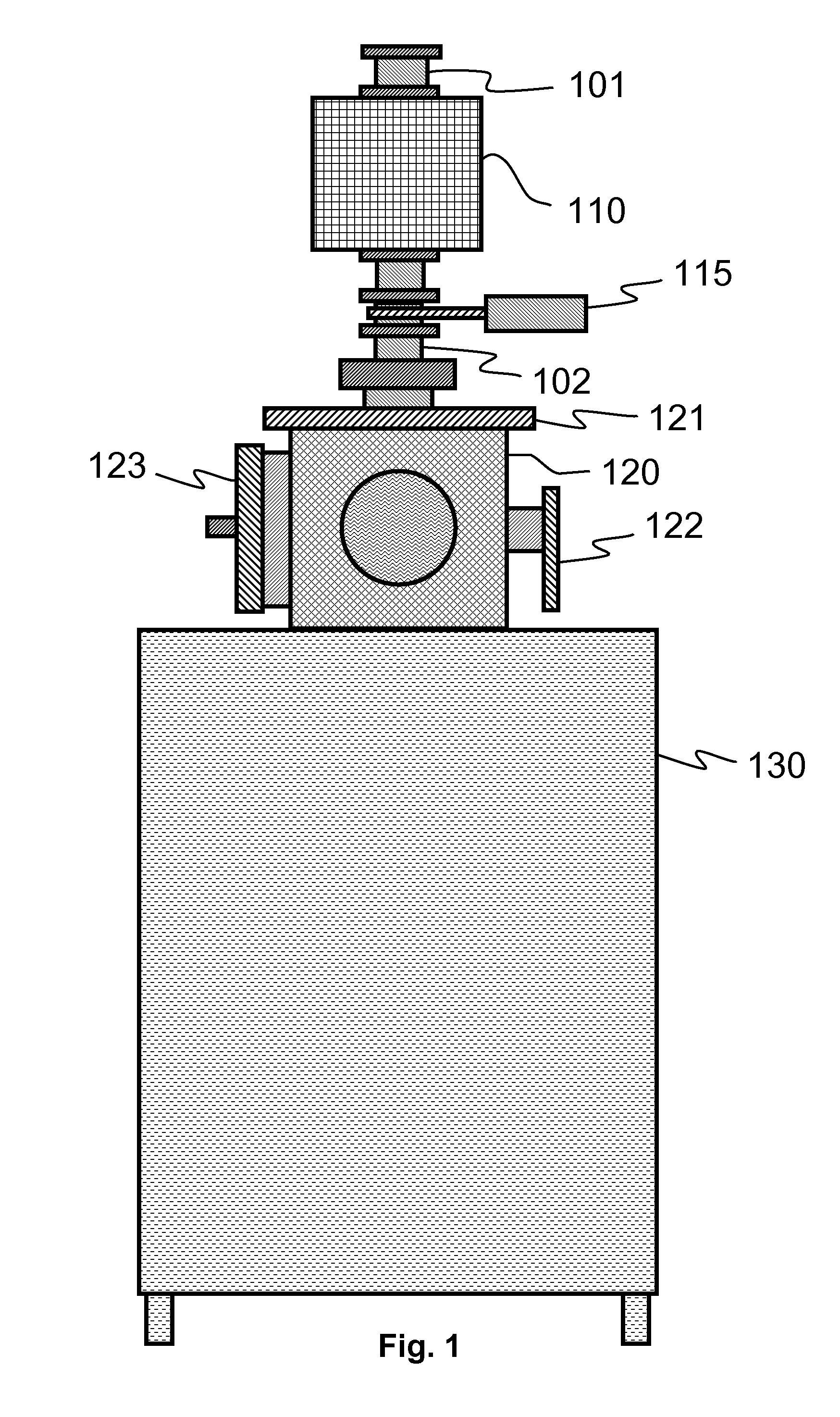
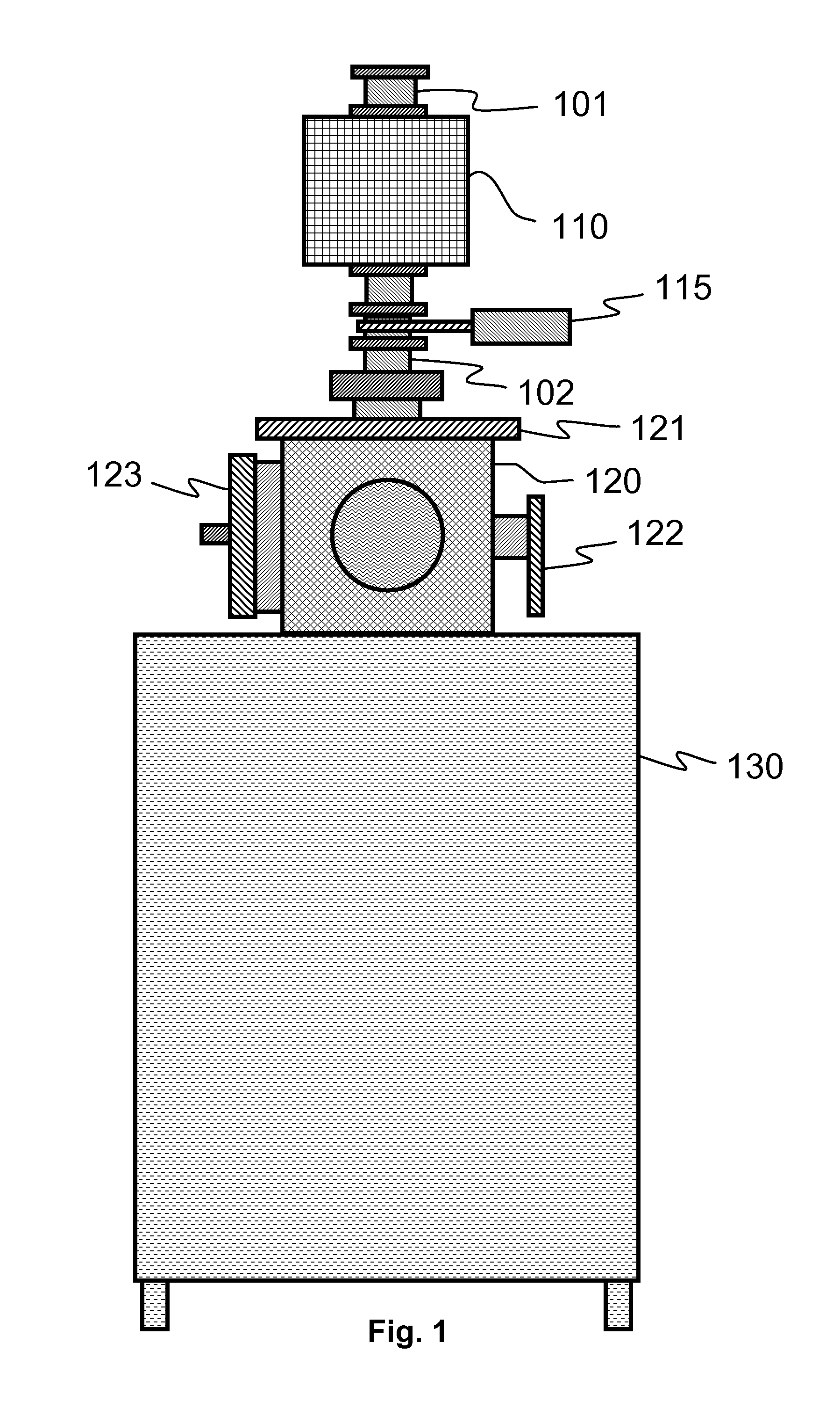
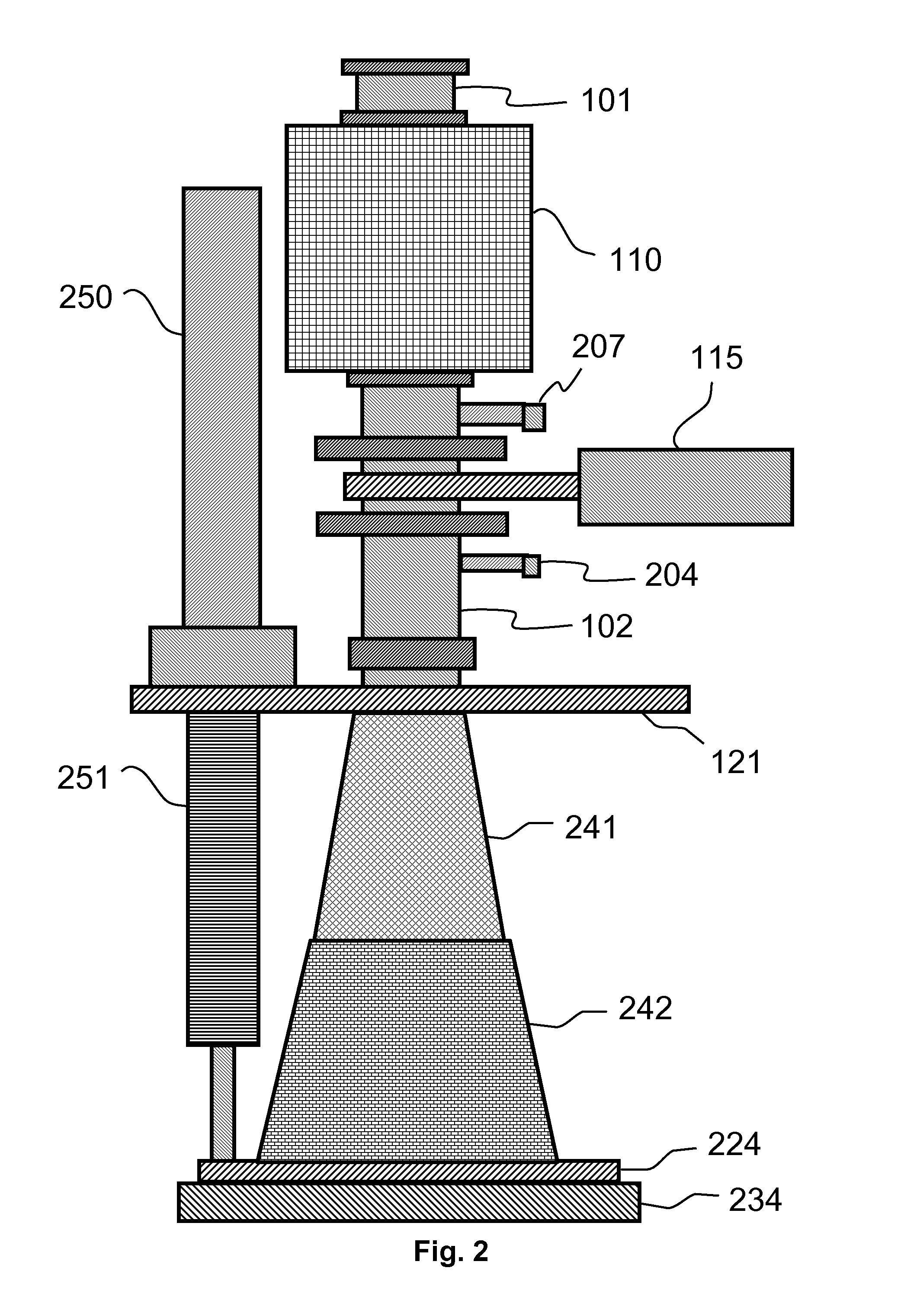
[0073]A 100-mm silicon wafer was loaded to the reaction chamber 335 with the dual elevator shown in FIG. 3. The instrumentation of the deposition reactor according to FIG. 6 and the timing diagram of FIG. 7 were used for growing aluminum oxide Al2O3 from trimethyl aluminum TMA and water H2O on the silicon wafer at 200° C. The flow rate of argon gas was 30 sccm through the carrier and purge gas line 101. The TMA pulse length was 0.1 s followed by the 6 s purge. Oxygen gas pulsing valve 414 was opened and 50 sccm of oxygen gas was flowing through the pulsing valve 414 to the remote plasma generator 110. The RF power was increased from 0 W to 2500 W to switch on the plasma and kept at the 2500 W level for 6 s. After that the RF power was lowered from 2500 W to 0 W to switch off the plasma. Next the oxygen gas valve was closed and the system was purged with inert gas for 10 s. The deposition cycle was repeated until a 36-nm Al2O3 thin film was grown. As a result, the 1-sigma non-uniform...


PUM

PropertyMeasurementUnit
Flow rateaaaaaaaaaa

Abstract

The invention relates to method including operating a plasma atomic layer deposition reactor configured to deposit material in a reaction chamber on at least one substrate by sequential self-saturating surface reactions, and allowing gas from an inactive gas source to flow into a widening radical in-feed part opening towards the reaction chamber substantially during a whole deposition cycle. The invention also relates to a corresponding apparatus.

Description

FIELD OF THE INVENTION[0001]The present invention generally relates to deposition reactors with a plasma source. More particularly, but not exclusively, the invention relates to such deposition reactors in which material is deposited on surfaces by sequential self-saturating surface reactions.BACKGROUND OF THE INVENTION[0002]Atomic Layer Epitaxy (ALE) method was invented by Dr. Tuomo Suntola in the early 1970's. Another generic name for the method is Atomic Layer Deposition (ALD) and it is nowadays used instead of ALE. ALD is a special chemical deposition method based on the sequential introduction of at least two reactive precursor species to a substrate. The substrate is located within a reaction space. The reaction space is typically heated. The basic growth mechanism of ALD relies on the bond strength differences between chemical adsorption (chemisorption) and physical adsorption (physisorption). ALD utilizes chemisorption and eliminates physisorption during the deposition proce...

Claims


Application Information

Patent Timeline
IPC IPC(8): B05C5/00H01L21/02
CPCB05C5/001H01L21/02274C23C16/403C23C16/45542C23C16/45544C23C16/45582H01J37/32357H01J37/32449H01J37/32743H01J37/32871C23C16/52
Inventor KILPI, VAINOLI, WEI-MINMALINEN, TIMOKOSTAMO, JUHANALINDFORS, SVEN
Owner PICOSUN OY
Why Eureka
Try Eureka