Sic single crystal, sic wafer, and semiconductor device

a semiconductor device and single crystal technology, applied in the direction of crystal growth process, crystal growth process, chemistry apparatus and processes, etc., can solve the problems of large number of defects, high dislocation density, threading screw dislocation, etc., to suppress the generation of stacking faults, reduce the number of basal plane dislocations exposed on the wafer surface, and reduce the number of dislocations succeeded by grown crystals or epitaxial films

Active Publication Date: 2014-01-30
TOYOTA CENT RES & DEV LAB INC
View PDF2 Cites 24 Cited by
  • Summary
  • Abstract
  • Description
  • Claims
  • Application Information

AI Technical Summary

Benefits of technology

[0028]When a wafer is cut out in nearly parallel to a {0001} plane from such an SiC single crystal, the number of basal plane dislocations exposed on the wafer surface reduces relatively. As a result, even when an SiC single crystal is grown by using such a wafer as a seed crystal or an epitaxial film is formed on the wafer surface, the number of dislocations succeeded by a grown crystal or an epitaxial film also reduces.
[0029]Further, when a semiconductor device is manufactured by using such an SiC single crystal, it is possible to suppress the generation of a stacking fault caused by the decomposition of a curved basal plane dislocation during use and the degradation of device characteristics caused by the generation of the stacking fault.

Problems solved by technology

The problem has, however, been that, in a single crystal obtained by the c-plane growth method, a large number of defects such as micro pipe defects (tubular voids about several μm to 100 μm in diameter) and threading screw dislocations (hereunder referred to also merely as “screw dislocations”) are generated in the direction parallel to the direction.
Further, a dislocation density is still high, intertwinement with a threading defect occurs frequently.
Furthermore, such a region is limited to a region of the order of submillimeters.

Method used


Image

  • Sic single crystal, sic wafer, and semiconductor device
  • Sic single crystal, sic wafer, and semiconductor device
  • Sic single crystal, sic wafer, and semiconductor device

Examples


example 1

[1. Preparation of Specimen]

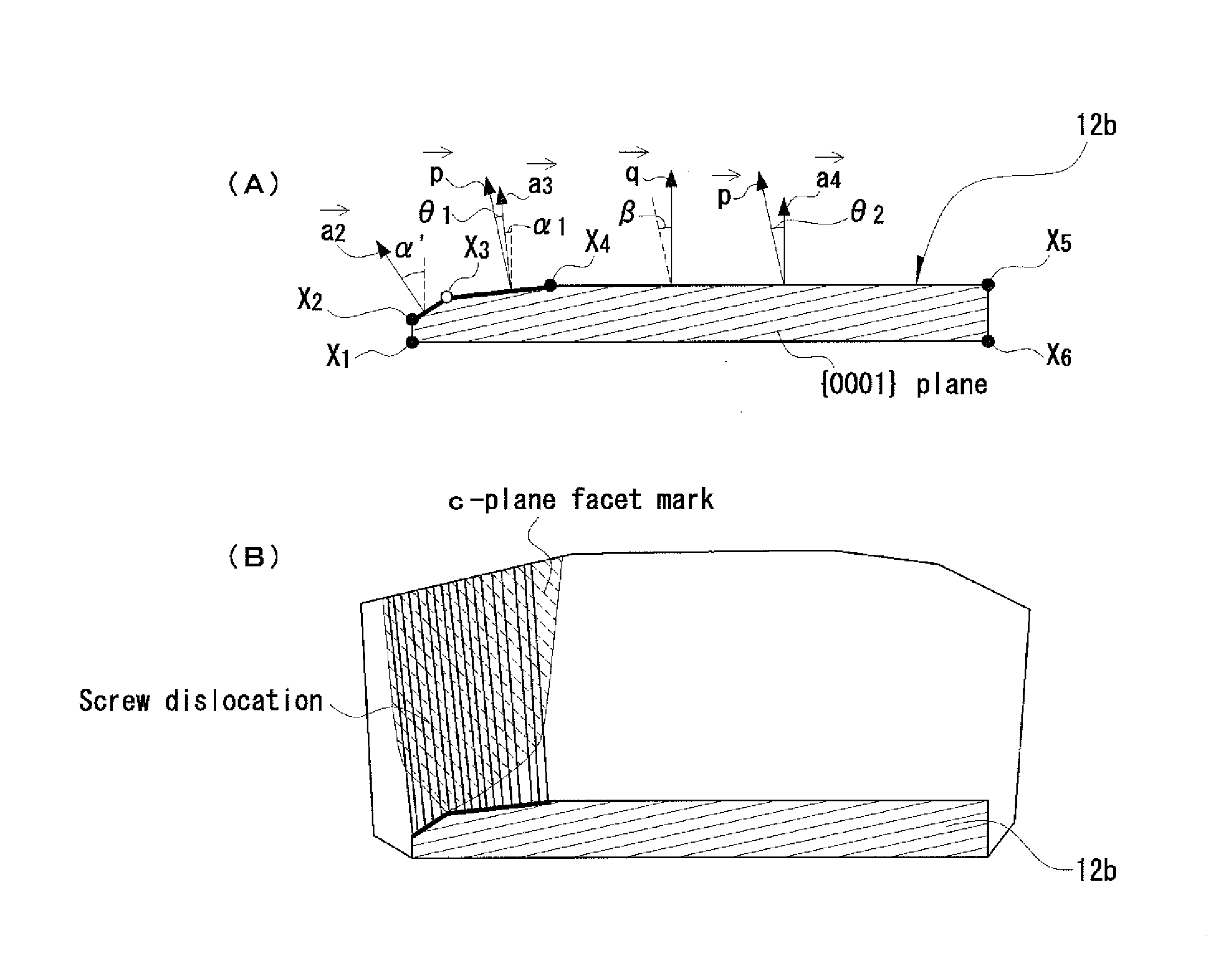
[0156]A step of growing an SiC single crystal on a growth plane nearly perpendicular to a c-plane, a step of taking out a seed crystal having a growth plane nearly perpendicular to both the last growth plane and the c-plane from the obtained SiC single crystal, and a step of growing an SiC single crystal again by using the seed crystal were repeated. A c-plane offset substrate was taken out from the obtained SiC single crystal and processed to the shape shown in FIG. 6A. A screw dislocation generation region was formed on the X2X3 plane and the X3X4 plane on the growth plane. By using it, an SiC single crystal was manufactured by a sublimation reprecipitation method. The obtained single crystal was cut in nearly parallel (offset angle: 8°) to a {0001} plane, flattening treatment and damaged layer removing treatment were applied to the surface, and thereby a wafer 500 μm in thickness was obtained. The damaged layer was removed by CMP treatment.

[2. Test Met...


PUM


Abstract

An SiC single crystal having at least one orientation region where a basal plane dislocation has a high linearity and is oriented to three crystallographically-equivalent <11-20> directions, and an SiC wafer and a semiconductor device which are manufactured from the SiC single crystal. The SiC single crystal can be manufactured by using a seed crystal in which the offset angle on a {0001} plane uppermost part side is small and the offset angle on an offset direction downstream side is large and growing another crystal on the seed crystal.

Description

FIELD OF THE INVENTION[0001]The present invention relates: to an SiC single crystal, an SiC wafer, and a semiconductor device; more specifically to an SiC single crystal having a highly-linear and highly-oriented basal plane dislocation, and an SiC wafer and a semiconductor device manufactured from such an SiC single crystal.BACKGROUND OF THE INVENTION[0002]In SiC (silicon carbide), a high-temperature type (α-type) having a hexagonal crystal structure and a low-temperature type (β-type) having a cubic crystal structure are known. SiC is characterized, in comparison with Si, by having a high thermal resistance, a broad band gap, and a high dielectric breakdown electric field strength. For that reason, a semiconductor including an SiC single crystal is expected as a candidate material of a next-generation power device substituting for an Si semiconductor. In particular, α-type SiC has a band gap broader than β-type SiC and hence the α-type SiC attracts attention as a semiconductor mat...

Claims


Application Information

Patent Timeline
Patent Type & Authority Applications(United States)
IPC IPC(8): H01L29/30H01L29/16
CPCH01L29/1608H01L29/30H01L29/045C30B23/025C30B29/36H01L29/861H01L29/32H01L21/02378H01L21/02433H01L21/02529H01L21/0254
Inventor GUNJISHIMA, ITARUURAKAMI, YASUSHIADACHI, AYUMU
Owner TOYOTA CENT RES & DEV LAB INC
Why Eureka
Try Eureka