Method and apparatus for correcting errors on a wafer processed by a photolithographic mask

a technology of photolithographic mask and mask, which is applied in the field of correcting errors on wafers processed by photolithographic masks, can solve the problems of increasing the difficulty of separating the various contributions of the overall overlay error, and reducing the difficulty of reducing the overlay error, so as to achieve the effect of minimizing the overlay error and reducing the difficulty of printing

Active Publication Date: 2014-02-06
CARL ZEISS SMS GMBH +1
View PDF9 Cites 40 Cited by
  • Summary
  • Abstract
  • Description
  • Claims
  • Application Information

AI Technical Summary

Benefits of technology

[0072]CDU error(s) in the sacrificial layer of a SADP process causes overlaylike error(s) in the final etched pattern. This effect is known as “pitch walking”. By in-die measurements of the spacer elements forming the etch mask, a variation

Problems solved by technology

It will be more and more difficult to separate the various contributions of the overall overlay error and to separately correct them.
Furthermore, the problems of the projection device of the photoli

Method used


Image

  • Method and apparatus for correcting errors on a wafer processed by a photolithographic mask
  • Method and apparatus for correcting errors on a wafer processed by a photolithographic mask
  • Method and apparatus for correcting errors on a wafer processed by a photolithographic mask

Examples


Embodiment Construction

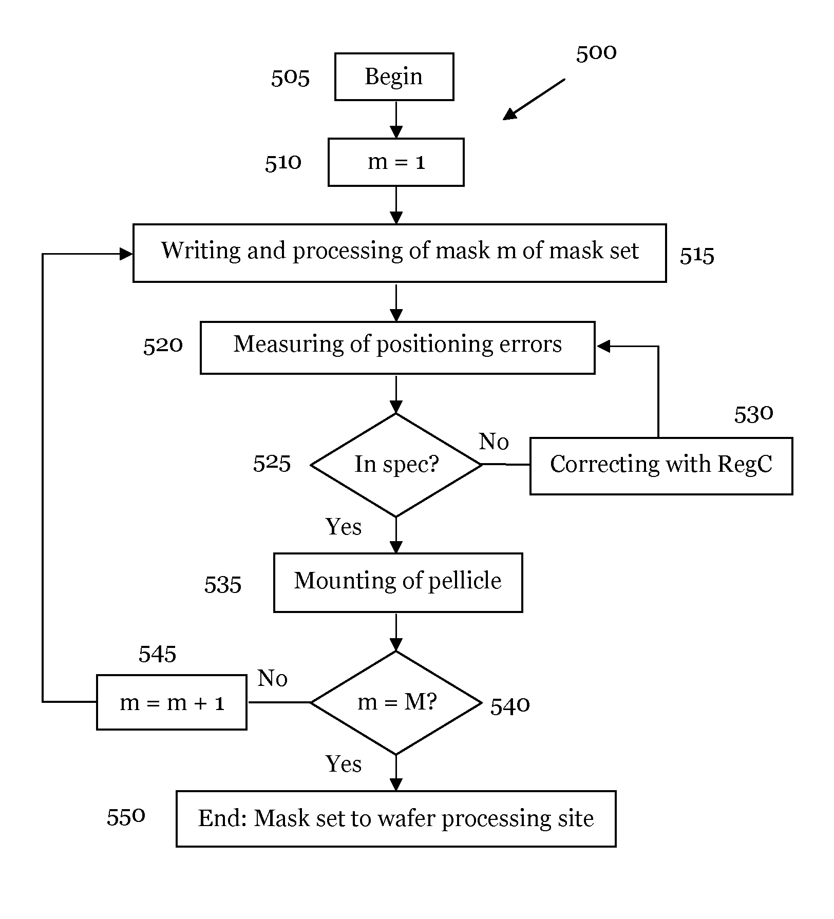
[0110]In the following, the present invention will be more fully described hereinafter with reference to the accompanying Figures, in which exemplary embodiments of the invention are illustrated. However, the present invention may be embodied in different forms and should not be construed as limited to the embodiments set forth herein. Rather, these embodiments are provided so that this disclosure will be thorough and will convey the scope of the invention to persons skilled in the art.

[0111]This first section describes an embodiment of the inventive method. To illustrate the inventive principle, differences are highlighted in the fabrication of a set of photolithographic masks with respect to the fabrication according the prior art. Further, these differences are also exemplified for a use case of a mask set. The inventive method is explained for the utilization of transmissive photolithographic masks. However, the person skilled in the art will appreciate that this is just an exam...


PUM


Abstract

The invention relates to a method for correcting at least one error on wafers processed by at least one photolithographic mask, the method comprises: (a) measuring the at least one error on a wafer at a wafer processing site, and (b) modifying the at least one photolithographic mask by introducing at least one arrangement of local persistent modifications in the at least one photolithographic mask.

Description

1. FIELD OF THE INVENTION[0001]The present invention relates to the field of correcting errors on a wafer processed by a photolithographic mask.2. BACKGROUND OF THE INVENTION[0002]As a result of the shrinking sizes of integrated circuits, photolithographic masks or templates of the nanoimprint lithography have to project smaller and smaller structures onto a photosensitive layer, i.e. a photo resist dispensed on a wafer. In order to fulfil this demand, the exposure wavelength of photolithographic masks has been shifted from the near ultraviolet across the mean ultraviolet into the far ultraviolet region of the electromagnetic spectrum. Presently, a wavelength of 193 nm is typically used for the exposure of the photo resist on wafers. In order to increase the resolution of the photolithographic exposure system water is often used as immersion liquid between the projection objective and the wafer. As a consequence, the manufacturing of photolithographic masks with increasing resolutio...

Claims


Application Information

Patent Timeline
IPC IPC(8): G03F1/72
CPCG03F1/72G03F1/84G03F7/7035G03F7/70466G03F7/70625G03F7/70633
Inventor BEYER, DIRKDMITRIEV, VLADIMIRSHARONI, OFIRWERTSMAN, NADAV
Owner CARL ZEISS SMS GMBH
Why Eureka
Try Eureka