Semiconductor memory device

a memory device and semiconductor technology, applied in information storage, static storage, digital storage, etc., can solve the problems of generating oxygen defects in the filament path, impaired reading sensitivity, and difficulty in reading, and achieve the effect of not reducing the rewriting operation speed

Inactive Publication Date: 2014-02-06
SHARP KK +1
View PDF0 Cites 70 Cited by
  • Summary
  • Abstract
  • Description
  • Claims
  • Application Information

AI Technical Summary

Benefits of technology

[0023]Accordingly, in some aspects, the present invention provides a method for efficiently rewriting a variable resistance element including metal oxide in a low-voltage and low-current operation, and a low-power consumption, large-capacity semiconductor memory device including the variable resistance element.
[0033]Preferably, each of the selection transistors has an on-resistance lower than at least an upper limit of the low-resistance range. More preferably, the on-resistance of each of the selection transistors is in a range of 10 kΩ or more to 100 kΩ or less. Therefore, a semiconductor memory device with high reading sensitivity and a large read margin may be achieved.
[0034]Preferably, the low-resistance range has an upper limit less than or equal to 100 kΩ, and the high-resistance range has a lower limit greater than or equal to 1 MΩ. Therefore, a semiconductor memory device having a resistance change ratio (the ratio of a resistance value in a high-resistance state to a resistance value in a low-resistance state) that is ten times or more larger than that in an existing semiconductor memory device and capable of facilitating the reading operation may be achieved.
[0035]According to an aspect of the present invention, simultaneously performing the set operation on a plurality of memory cells may substantially reduce the issue of a reduction in operation speed which is caused by taking a certain amount of time to perform the set operation. The set operation performed with the limitation of a set current to a certain value or less may not lead to a reduction in the rewriting operation speed even though the application of a set voltage pulse for a short time is insufficient for conversion to a low resistance. Conversion to a low resistance may be performed by applying the set voltage pulse for a long time.
[0037]Therefore, a low-power-consumption, high-capacity semiconductor memory device capable of performing low-voltage and low-current rewriting without reducing the rewriting operation speed may be achieved.

Problems solved by technology

However, the current memory devices described above have their merits and demerits, and the developers are facing many difficulties in realizing ideal “universal memory” combining the respective benefits of static RAM (SRAM), dynamic RAM (DRAM), and flash memory.
In the case of switching to the low-resistance state, in contrast, a voltage pulse is applied so that the electrode with a larger work function has a negative polarity, thereby generating oxygen defects in the filament path.
For this reason, the reading sensitivity is impaired and difficulties occur in reading unless the resistance value of the variable resistance element in the low-resistance state is set sufficiently higher than the on-resistance of the transistor.
In this case, a reduction in the amount of voltage and electric current applied in the set operation or the time during which electric current flows may cause incomplete movement of oxygen, resulting in a discontinuous filament path being formed.
Thus, the smaller the set current is, the narrower the filament path to be formed is, resulting in concentration of the Joule heat generated in the filament path.

Method used


Image

  • Semiconductor memory device
  • Semiconductor memory device
  • Semiconductor memory device

Examples


first embodiment

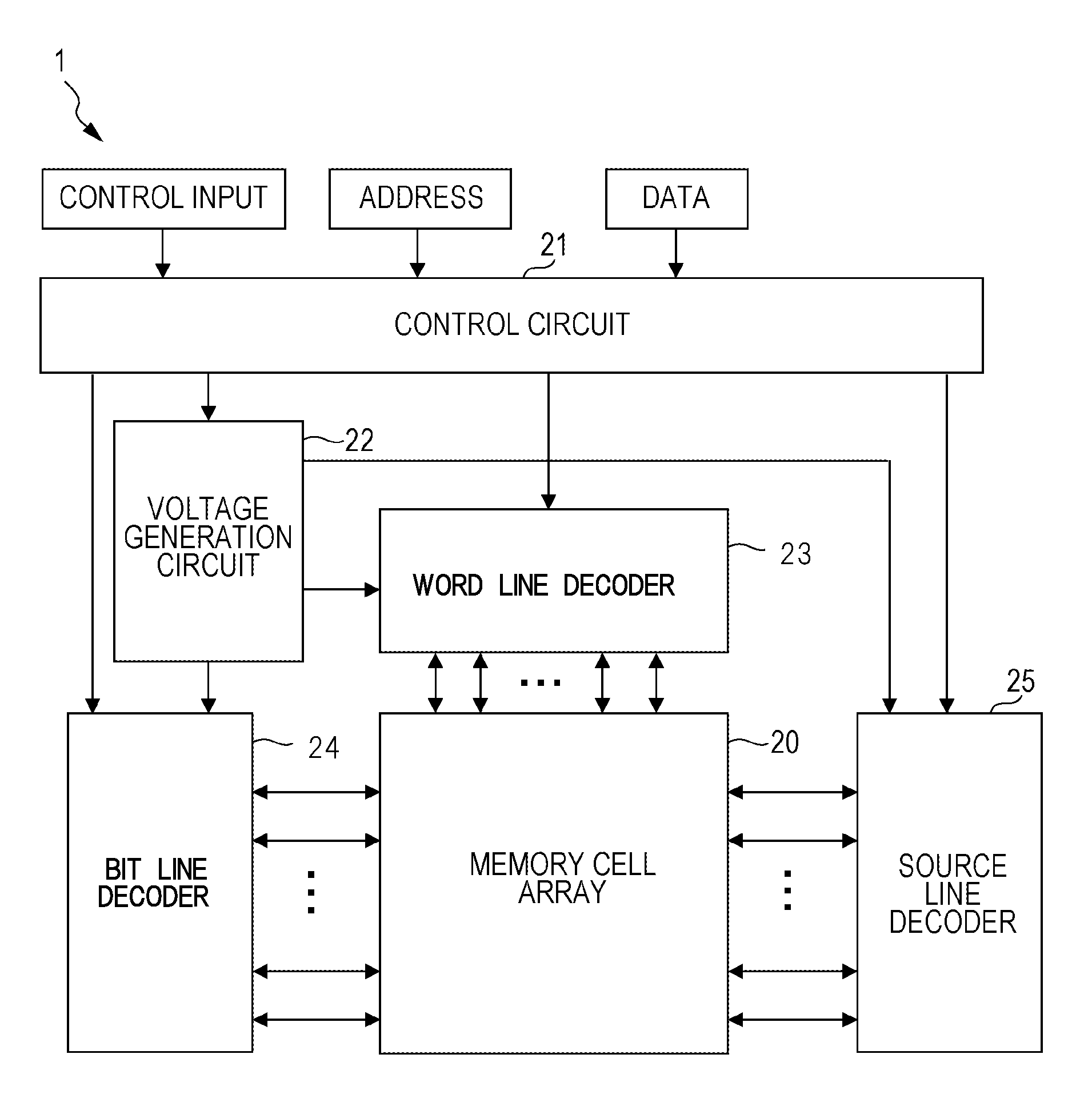
[0047]FIG. 1 illustrates a circuit block diagram illustrating a schematic configuration of a semiconductor memory device according to an embodiment of the present invention. Referring to FIG. 1, a semiconductor memory device 1 includes a memory cell array 20, a control circuit 21, a voltage generation circuit 22, a word line decoder 23, a bit line decoder 24, and a source line decoder 25.

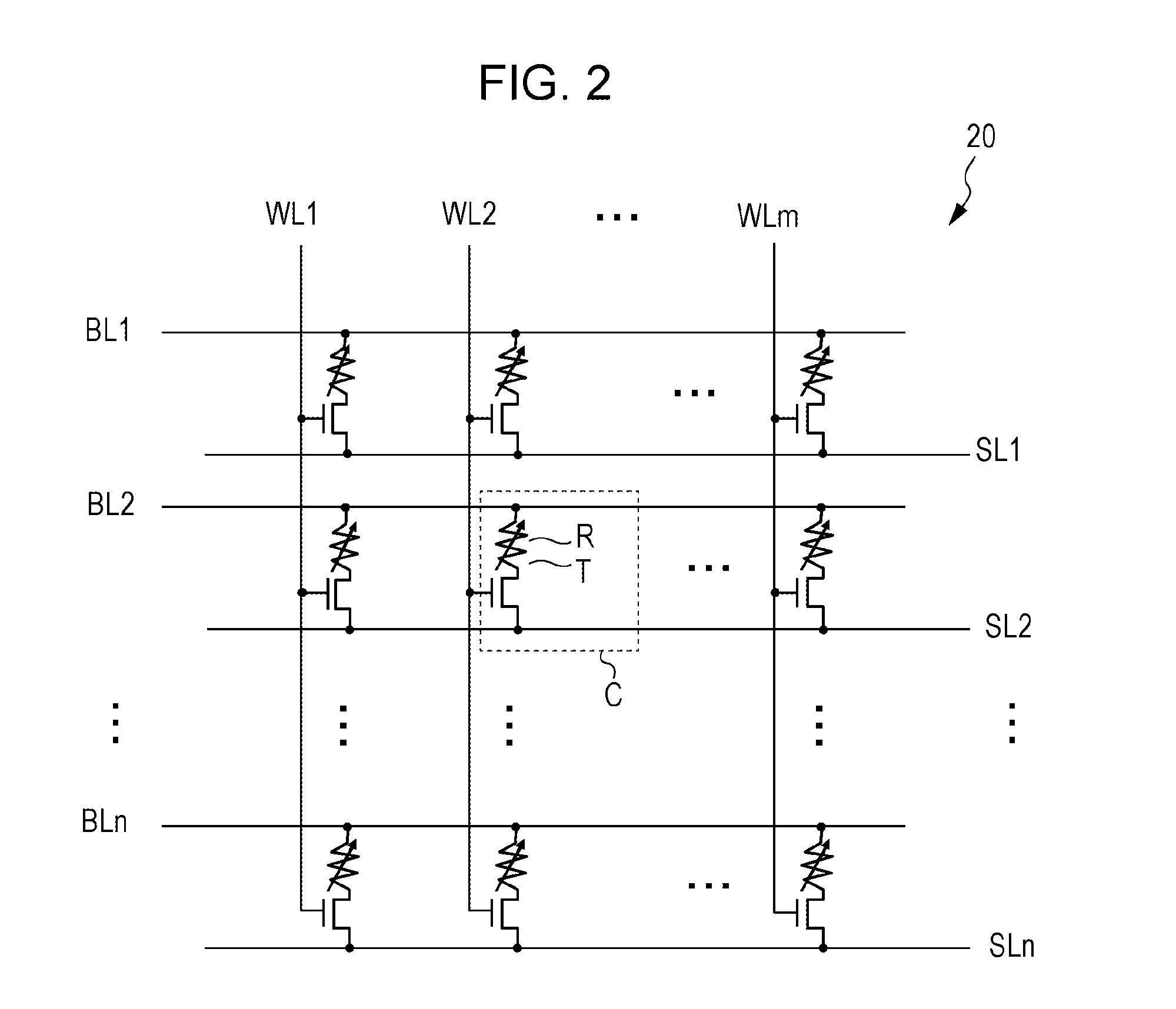
[0048]FIG. 2 illustrates an example of a circuit configuration of the memory cell array 20. As illustrated in FIG. 2, the memory cell array 20 has a plurality of memory cells C arranged in row and column directions. Each of the memory cells C has a pair of input and output terminals (hereinafter referred to as an “input-output terminal pair”) in which a variable resistance element R and a selection transistor T are connected in series. In the respective memory cells C, first ends on the variable resistance element R side of the input-output terminal pairs are connected to a plurality of bit lines BL...

second embodiment

[0076]In the first embodiment, a description has been given of a method for reducing the time required for the set operation per memory cell by executing the set operation by applying a set voltage pulse to a selected memory cell for a long time while the set voltage pulse is applied simultaneously to a plurality of selected memory cells, thereby substantially reducing the time required for rewriting. It is still more preferable that the time during which the set voltage pulse is applied be shorter.

[0077]As the time during which the set voltage pulse is applied is reduced, however, the resistance value of a variable resistance element after the set operation is deviated from the low-resistance range, and the number of elements for which the set operation has failed increases.

[0078]The duration of the set operation may be reduced by, after the set operation, reading the resistance states of the variable resistance elements of selected memory cells and performing the set operation aga...

third embodiment

[0085]In the semiconductor memory device 1, the memory cell array 20 may include a plurality of banks. FIG. 6 illustrates an example of a semiconductor memory device configured such that a memory cell array includes a plurality of banks. Referring to FIG. 6, a semiconductor memory device 2 includes a memory cell array 20 that is divided into four banks 20a to 20d. Each of the banks 20a to 20d corresponds to the memory cell array 20 of the semiconductor memory device 1, and a plurality of memory cells arranged in a matrix are connected through the word lines WL1 to WLm, the bit lines BL1 to BLn, and the source lines SL1 to SLn. Similarly to the semiconductor memory device 1, the semiconductor memory device 2 includes a control circuit 21, a voltage generation circuit 22 (not illustrated), word line decoders 23, bit line decoders 24, and source line decoders 25. In FIG. 6, for the sake of simplicity, a set of decoders including each of the word line decoders 23, each of the bit line d...


PUM


Abstract

A semiconductor memory device includes a memory cell array having a plurality of memory cells arranged in a matrix, each memory cell being configured such that a variable resistance element and a selection transistor are connected in series. A set operation for a memory cell (an operation of converting the resistance of the variable resistance element to a low resistance) is performed by applying a set voltage pulse for a longer time than that for a reset operation (an operation of converting the resistance of the variable resistance element to a high resistance) while limiting, using the selection transistor, an electric current flowing in the set operation to a certain low electric current, and by simultaneously applying the set voltage pulse to the plurality of memory cells.

Description

CROSS REFERENCE TO RELATED APPLICATION[0001]This Nonprovisional application claims priority under 35 U.S.C. §119(a) on Patent Application No. 2012-173091 filed in Japan on Aug. 3, 2012 the entire contents of which are hereby incorporated by reference.BACKGROUND OF THE INVENTION[0002]1. Field of the Invention[0003]The present invention relates to non-volatile semiconductor devices for storing information using non-volatile variable resistance elements, and more specifically to a semiconductor memory device which allows efficient writing and erasing of data and a control method for the semiconductor memory device.[0004]2. Description of the Related Art[0005]In recent years, there have been proposed high-speed operable next-generation non-volatile random access memory (NVRAM) devices that might replace flash memories and that have various device structures, such as a ferroelectric RAM (FeRAM), a magnetic RAM (MRAM), and an ovonic unified memory (OUM), and there is fierce development co...

Claims


Application Information

Patent Timeline
Patent Type & Authority Applications(United States)
IPC IPC(8): G11C13/00
CPCG11C13/0021G11C13/0069G11C2213/79G11C13/0007
Inventor ISHIHARA, KAZUYATAMAI, YUKIONAKANO, TAKASHISEKO, AKIYOSHI
Owner SHARP KK
Why Eureka
Try Eureka