

Polishing pad and manufacturing method therefor
a polishing pad and manufacturing method technology, applied in the field of polishing pads, can solve the problems of unsatisfactory dry polishing pads in terms of reducing the scars (scratches) formed on the surface of workpieces, and still hard, etc., to achieve the effect of suppressing strong pressing, low storage elastic modulus, and moderate dressing properties
- Summary
- Abstract
- Description
- Claims
- Application Information
AI Technical Summary
Benefits of technology
Problems solved by technology
Method used
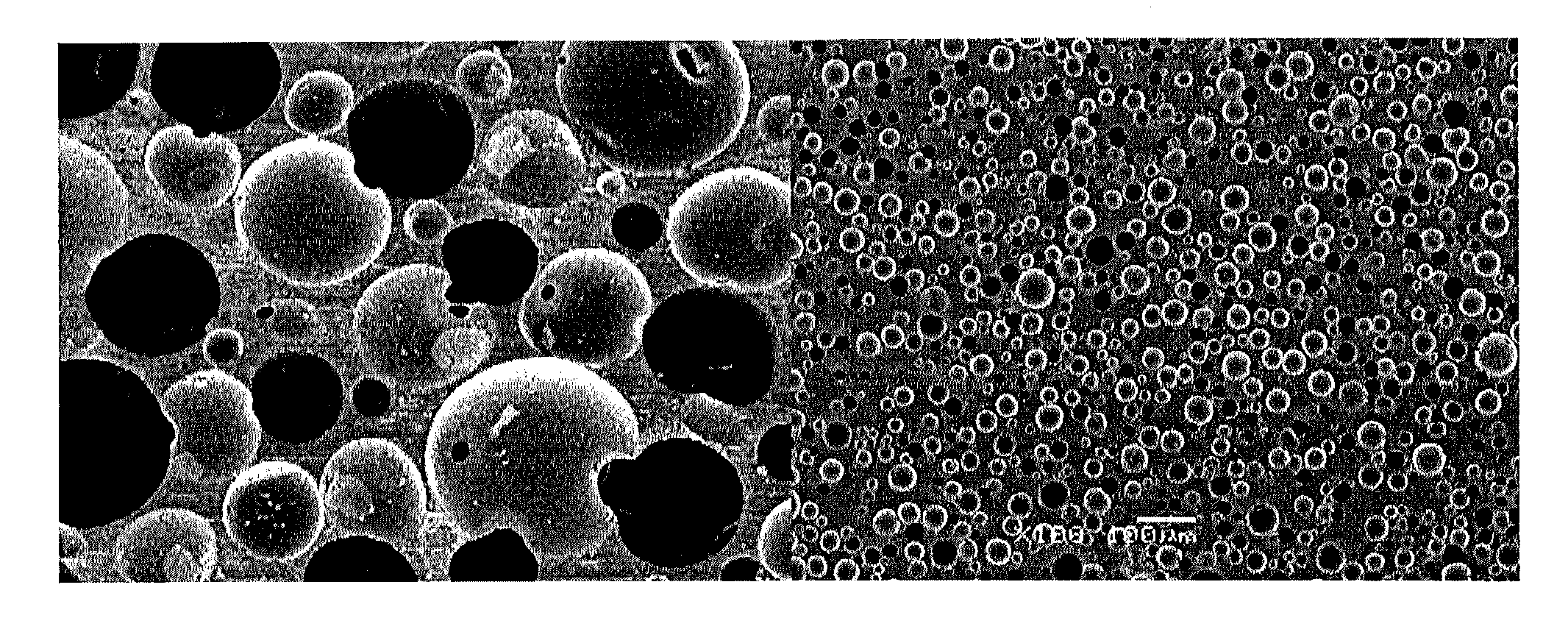
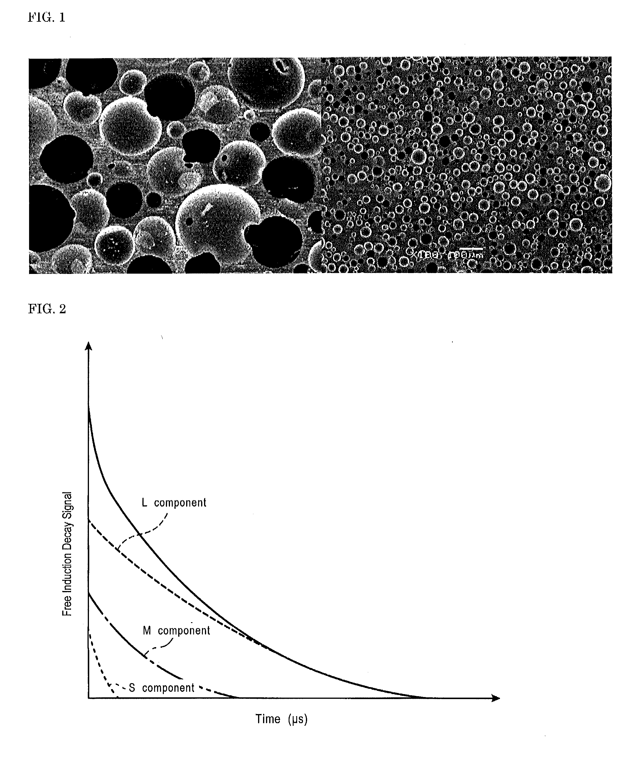
Image

Examples
example 1
[0155]In Example 1, as a first component, which was a prepolymer, an isocyanate group-containing urethane prepolymer having an isocyanate content of 7.8% and an NCO equivalent weight of 540 was used. The prepolymer was obtained by reacting 2,4-TDI (286 parts) and the PTMG (714 parts) having a number average molecular weight of approximately 1000. This prepolymer was heated to 55° C., and degassed under reduced pressure. As a second component, which was a chain extender, solid MOCA was used. The solid MOCA was melt at 120° C., and degassed under reduced pressure. A third component, an aqueous dispersion, was obtained by mixing the three-functional PPG (42 parts) having a number average molecular weight of 3000, water (3 parts), a catalyst (TOYOCAT-ET manufactured by Tosoh Corporation) (1 part), a silicone-based surfactant (SH-193 manufactured by Dow Corning Corporation) (1 part) with each other at 35° C. for 1 hour with stirring. Then, the aqueous dispersion was degassed under reduce...
example 5
[0158]In Example 5, as a first component, which was a prepolymer, an isocyanate group-containing urethane prepolymer having an isocyanate content of 7.8% and an NCO equivalent weight of 540 was used. The prepolymer was obtained by reacting 2,4-TDI (286 parts) and the PTMG (714 parts) having a number average molecular weight of approximately 1000. This prepolymer was heated to 55° C., and degassed under reduced pressure. As a second component, which was a chain extender, the liquid MOCA (234 parts) was degassed under reduced pressure. A third component, an aqueous dispersion, was obtained by mixing the three-functional PPG (41 parts) having a number average molecular weight of 3000, water (3 parts), a catalyst (TOYOCAT-ET manufactured by Tosoh Corporation) (1 part), and a silicone-based surfactant (SH-193 manufactured by Dow Corning Corporation) (4 parts) with each other with stirring. Then, the aqueous dispersion was degassed under reduced pressure. The first component, the second c...
example 10
[0161]In Example 10, as a first component, which was a prepolymer, an isocyanate group-containing urethane prepolymer having an isocyanate content of 10.0% and an NCO equivalent weight of 420 was used. The prepolymer was obtained by reacting 2,4-TDI (325 parts) and the PTMG (675 parts) having a number average molecular weight of approximately 1000. This prepolymer was heated to 55° C., and degassed under reduced pressure. As a second component, which was a chain extender, the liquid MOCA (397 parts) was degassed under reduced pressure. A third component, an aqueous dispersion, was obtained by mixing the three-functional PPG (43 parts) having a number average molecular weight of 3000, water (1 part), a catalyst (TOYOCAT-ET manufactured by Tosoh Corporation) (1 part), and a silicone-based surfactant (SH-193 manufactured by Dow Corning Corporation) (4 parts) with each other with stirring. Then, the aqueous dispersion was degassed under reduced pressure. The first component, the second ...
PUM
| Property | Measurement | Unit |
|---|---|---|
| Temperature | aaaaa | aaaaa |
| Fraction | aaaaa | aaaaa |
| Percent by mass | aaaaa | aaaaa |
Abstract
Description
Claims
Application Information