Formation method of oxide semiconductor film

a technology of oxide semiconductor film and formation method, which is applied in the direction of semiconductor devices, basic electric elements, electrical appliances, etc., can solve the problems of difficult to secure the reliability of such a transistor, amorphous oxide semiconductor film, unstable physical properties, etc., and achieve high crystallinity

Inactive Publication Date: 2014-02-13
SEMICON ENERGY LAB CO LTD
View PDF3 Cites 15 Cited by
  • Summary
  • Abstract
  • Description
  • Claims
  • Application Information

AI Technical Summary

Benefits of technology

[0019]According to one embodiment of the present invention, an oxide semiconductor film with high crystallinity can be formed.

Problems solved by technology

Although a transistor including an oxide semiconductor film can obtain transistor characteristics relatively with ease, the oxide semiconductor film is likely to be amorphous and has unstable physical properties.
Thus, it is difficult to secure reliability of such a transistor.

Method used


Image

  • Formation method of oxide semiconductor film
  • Formation method of oxide semiconductor film
  • Formation method of oxide semiconductor film

Examples


embodiment 1

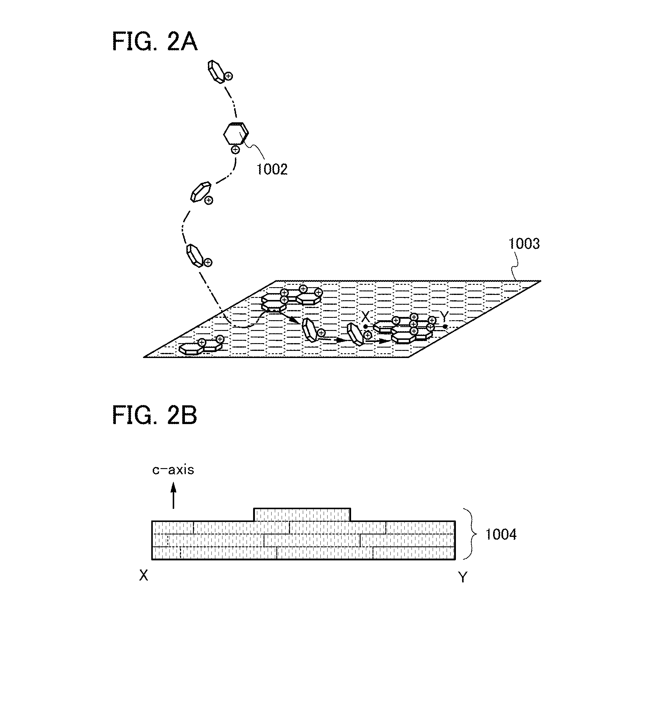
[0037]In this embodiment, a film formation method of an oxide semiconductor film of one embodiment of the present invention will be described with reference to FIGS. 1A and 1B, FIGS. 2A and 2B, FIGS. 3A and 3B, and FIG. 4.

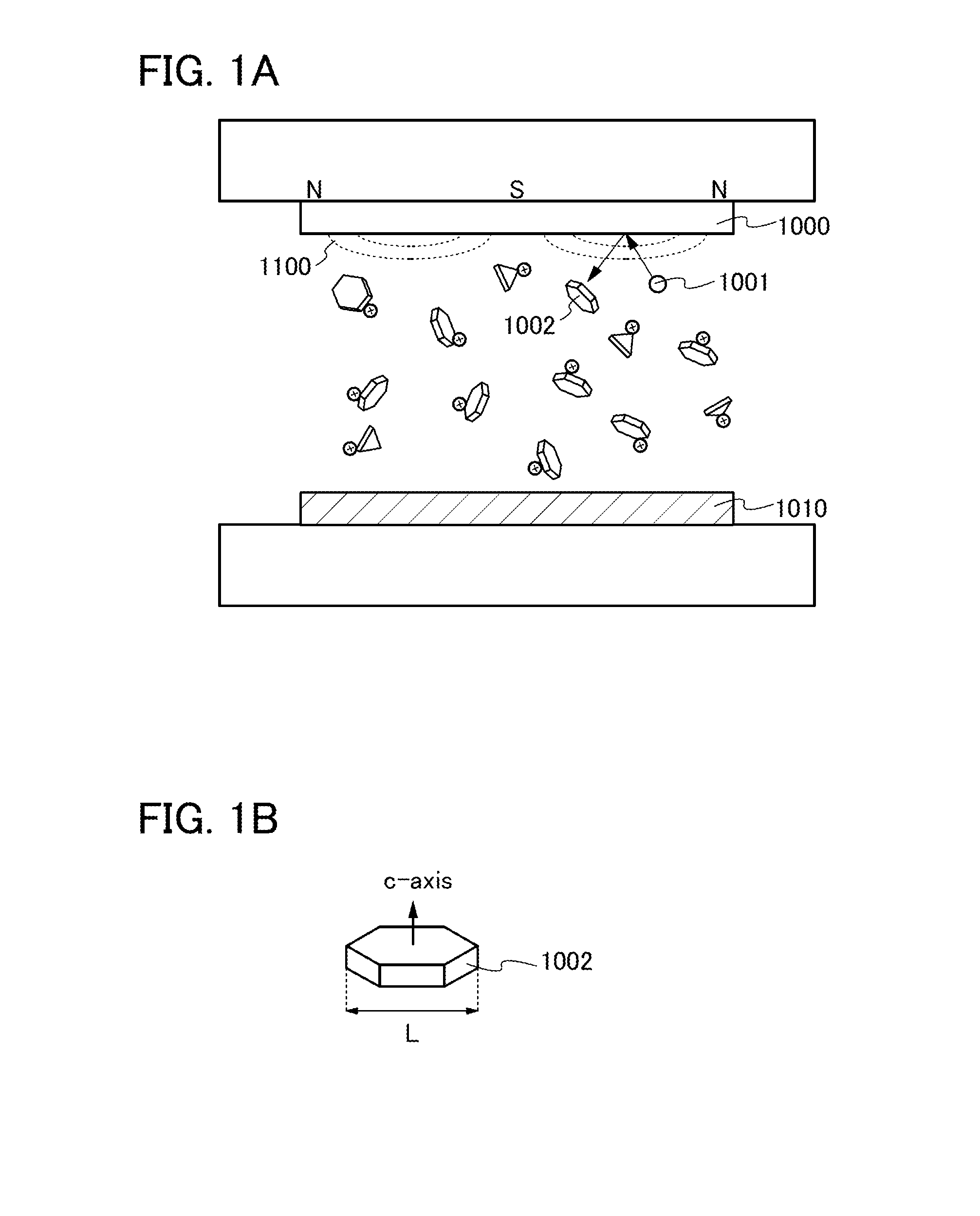
[0038]FIG. 1A is a schematic diagram illustrating a state in which an ion 1001 collides with a sputtering target 1000 to separate crystalline sputtered particles 1002 from the sputtering target 1000 and the crystalline sputtered particles 1002 are transferred to a substrate 1010 having a deposition surface.

[0039]FIG. 1A illustrates the case of using a DC magnetron sputtering method, in which case a magnet is provided inside or outside a target support for supporting the sputtering target 1000. In this structure, a semi-circular magnetic force line 1100 is generated on the sputtering target 1000. With the magnet, high-density plasma can be confined in the periphery of the sputtering target 1000, so that improvement in deposition rate and a reduction in plasma damage...

embodiment 2

[0076]In this embodiment, a sputtering target which can be used for forming an oxide semiconductor film of one embodiment of the present invention will be described.

[0077]FIG. 5 illustrates an example of a fabrication process of a sputtering target.

[0078]First, raw materials are weighed and are mixed in a predetermined molar ratio (step S101).

[0079]In this embodiment, description is given on the case where an oxide powder containing In, M, and Zn (also referred to as an In-M-Zn oxide powder) is obtained as the oxide powder containing a plurality of metal elements.

[0080]Specifically, an InOX oxide powder, a MOY oxide powder, and a ZnOZ oxide powder are prepared and mixed in a predetermined molar ratio. Note that X, Y, and Z are each a given positive number; for example, X, Y, and Z are 1.5, 1.5, and 1, respectively.

[0081]It is needless to say that the above oxide powders are examples, and oxide powders can be selected as appropriate in order to obtain a desired composition. Note that...

embodiment 3

[0098]In this embodiment, a structure example of a transistor to which the oxide semiconductor film described in Embodiment 1 is applied will be described with reference to drawings.

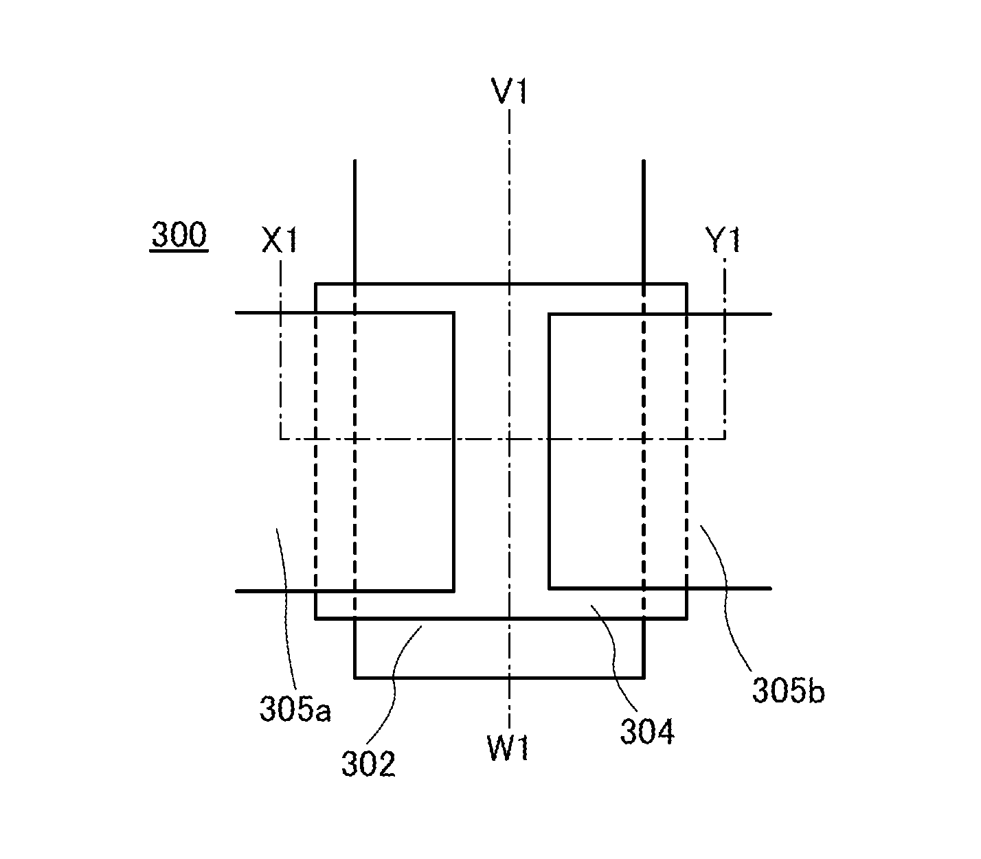
[0099]FIGS. 6A to 6C illustrate a structure example of a transistor 300. The transistor 300 exemplified by this structure example is a bottom-gate transistor. FIG. 6A is a plan view of the transistor 300, FIG. 6B is a cross-sectional view taken along line X1-Y1 in FIG. 6A, and FIG. 6C is a cross-sectional view taken along line V1-W1 in FIG. 6A.

[0100]The transistor 300 includes a gate electrode layer 302 over a substrate 301, an insulating layer 303 over the substrate 301 and the gate electrode layer 302, an oxide semiconductor film 304 over the insulating layer 303, which overlaps with the gate electrode layer 302, and a source electrode layer 305a and a drain electrode layer 305b which are in contact with the top surface of the oxide semiconductor film 304. Moreover, an insulating layer 306 covers the i...


PUM

PropertyMeasurementUnit
temperatureaaaaaaaaaa
diameteraaaaaaaaaa
lengthaaaaaaaaaa

Abstract

An oxide semiconductor film with high crystallinity is formed. An ion is made to collide with a sputtering target including a polycrystalline oxide containing a plurality of crystal grains to separate parts of the plurality of crystal grains and obtain flat plate-like sputtered particles, and the flat plate-like sputtered particles are deposited on a substrate having an insulating surface, which is heated at a temperature higher than 400° C. and lower than or equal to 500° C., to form an oxide semiconductor film including a crystal part over the substrate. Since the substrate which is a deposition surface is heated at a high temperature, the flat plate-like sputtered particles are rearranged and thus the oxide semiconductor film has a high film density.

Description

BACKGROUND OF THE INVENTION[0001]1. Field of the Invention[0002]The invention disclosed in this specification relates to a semiconductor device and a fabrication method thereof. The present invention particularly relates to an oxide semiconductor film included in a semiconductor device and a film formation method thereof.[0003]Note that a semiconductor device in this specification and the like refers to any device which can function by utilizing semiconductor characteristics, and electro-optical devices, semiconductor circuits, and electronic devices are all semiconductor devices.[0004]2. Description of the Related Art[0005]A technique by which a transistor is formed using a semiconductor thin film formed over a substrate having an insulating surface has been attracting attention. The transistor is applied to a wide range of electronic devices such as an integrated circuit (IC) or an image display device (also simply referred to as a display device). As a semiconductor thin film app...

Claims


Application Information

Patent Timeline
Patent Type & Authority Applications(United States)
IPC IPC(8): H01L21/02
CPCH01L21/02595H01L21/02554H01L21/02565H01L21/02631H01L27/11807H01L29/7869H01L29/04H01L29/66969H10B41/70
Inventor YAMAZAKI, SHUNPEI
Owner SEMICON ENERGY LAB CO LTD
Why Eureka
Try Eureka