
Opto-Electric Device and Method of Manufacturing an Opto-Electric Device

a technology of opto-electric devices and opto-electric devices, which is applied in the field of opto-electric devices, can solve the problems of not disclosing the combination of cusslers, and achieve the effects of improving the efficiency of the getter, reducing the lag time of water, and quick diffusion

Inactive Publication Date: 2014-02-20
NEDERLANDSE ORG VOOR TOEGEPAST-NATUURWETENSCHAPPELIJK ONDERZOEK (TNO) +2
View PDF1 Cites 24 Cited by
  • Summary
  • Abstract
  • Description
  • Claims
  • Application Information

AI Technical Summary

Benefits of technology

The patent text describes a technology that helps prevent moisture or other substances from reaching the opto-electric element in a device. This is achieved by using a layer called a lateral diffusion layer, which allows the substances to diffuse laterally over a larger area before reaching the getter layer. This getter layer can more efficiently catch the substances and prevent them from reaching the structure underneath. The technology also results in better use of the getter capacity and allows for a longer time for moisture to reach the structure. Additionally, the patent describes a method where a planarization layer can be used to prevent non-aligned particles from protruding the inorganic layer.

Problems solved by technology

After the getter in this semi-circle is saturated the water can reach the underlying structure leading to degradation.
However, Cussler does not disclose the combination wherein a lateral diffusion layer is arranged between an inorganic layer and a layer having a getter function.

Method used


Image

  • Opto-Electric Device and Method of Manufacturing an Opto-Electric Device
  • Opto-Electric Device and Method of Manufacturing an Opto-Electric Device
  • Opto-Electric Device and Method of Manufacturing an Opto-Electric Device

Examples


Embodiment Construction

[0047]In the following detailed description numerous specific details are set forth in order to provide a thorough understanding of the present invention. However, it will be understood by one skilled in the art that the present invention may be practiced without these specific details. In other instances, well known methods, procedures, and components have not been described in detail so as not to obscure aspects of the present invention.

[0048]The invention is described more fully hereinafter with reference to the accompanying drawings, in which embodiments of the invention are shown. This invention may, however, be embodied in many different forms and should not be construed as limited to the embodiments set forth herein. Rather, these embodiments are provided so that this disclosure will be thorough and complete, and will fully convey the scope of the invention to those skilled in the art. In the drawings, the size and relative sizes of layers and regions may be exaggerated for c...


PUM


Abstract

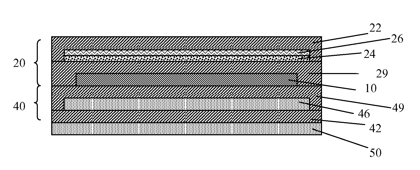
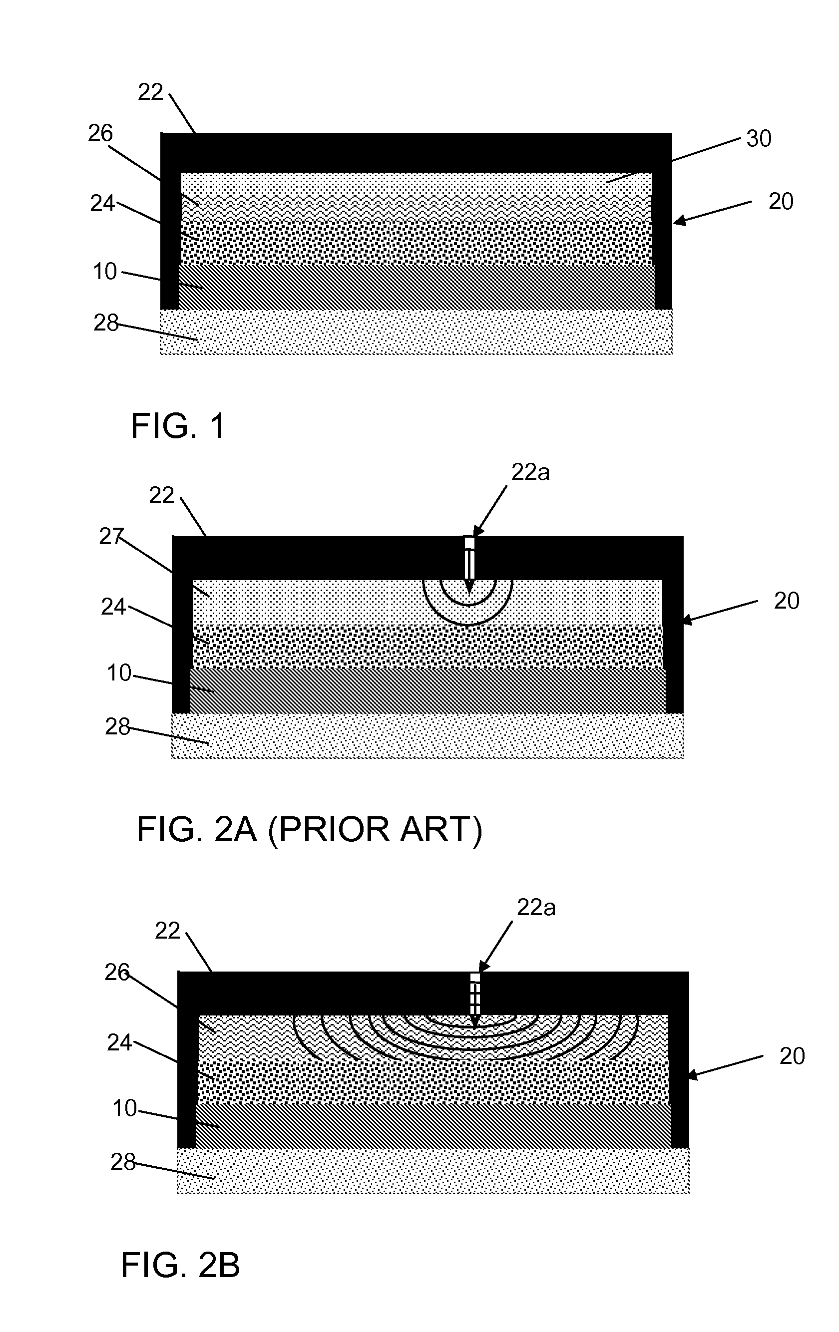
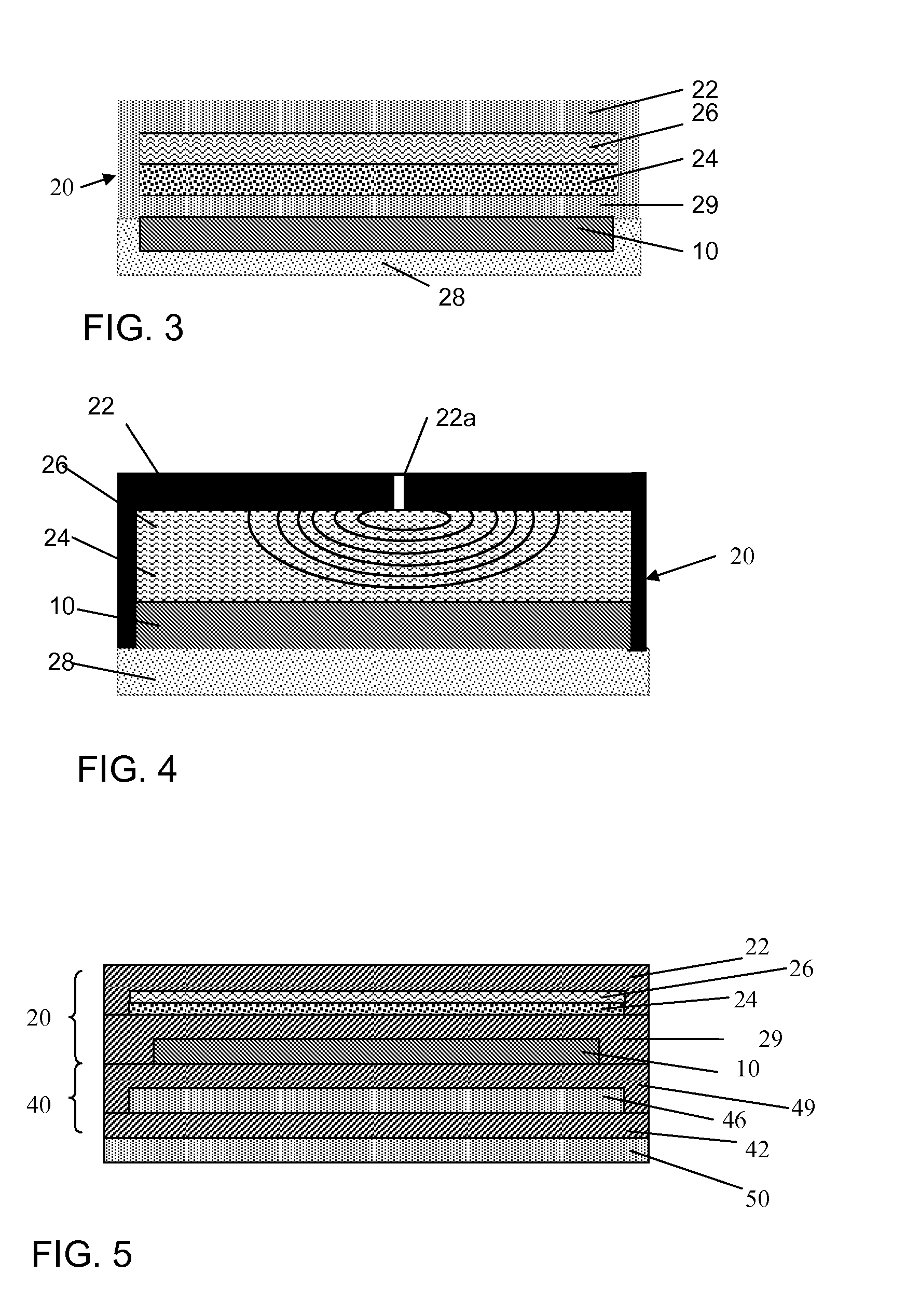
An opto-electric device is presented that comprises an opto-electric element (10) enclosed by a barrier structure (20) for inhibiting a transmission of moisture from an environment towards the opto-electric element. The barrier structure includes a stack of layers comprising at least an inorganic layer (22) and a moisture getter material in a layer arranged between the inorganic layer and the opto-electric element. The stack includes a lateral diffusion layer (26), wherein the getter material is present in a separate getter layer (24) arranged between the opto-electric element (10) and the lateral diffusion layer (26) and / or the getter material is present in the lateral diffusion layer (26).

Description

BACKGROUND[0001]1. Field of the Invention[0002]The present invention relates to an opto-electric device.[0003]The present invention further relates to a method of manufacturing an opto-electric device.[0004]2. Related Art[0005]A new generation of organic thin film based devices, such as organic light-emitting diodes (OLEDs) for lighting and displays, thin film batteries, thin film organic solar cells, electrochromic foils, electrophoretic displays, etc., have the potential to become a next revolution in electronic systems.[0006]An OLED comprises a light-emitting organic film that is formed between an electrode and a counter electrode. Usually the light-emitting organic film is part of a stack that may comprise additional layers, such as a hole transport layer, an electron block layer, an electron transport layer and a luminescent layer.[0007]Various materials applied in OLEDs and other organic devices are sensitive to substances as moisture in the atmosphere. Accordingly a protectio...

Claims


Application Information

Patent Timeline
Patent Type & Authority Applications(United States)
IPC IPC(8): G02B1/10
CPCG02B1/105H10K50/846H10K2102/331H10K2102/351G02B1/14H10K50/8445H10K50/844
Inventor VAN MOL, ANTONIUS MARIA BERNARDUSVAN DE WEIJER, PETERKOTZEV, DIMITER LUBOMIROV
Owner NEDERLANDSE ORG VOOR TOEGEPAST-NATUURWETENSCHAPPELIJK ONDERZOEK (TNO)
Learn More