Conductive material, bonding method using the same, and bonded structure

a technology of conductive materials and bonding methods, applied in the direction of connection contact material, application, soldering apparatus, etc., can solve the problems of low reliability, unusable products to be bonded, and reduced bonding strength of the solvent paste in which sn remains, etc., to achieve excellent strength, high bonding reliability, and short time

Active Publication Date: 2013-09-12
MURATA MFG CO LTD
View PDF3 Cites 30 Cited by
  • Summary
  • Abstract
  • Description
  • Claims
  • Application Information

AI Technical Summary

Benefits of technology

[0013]The present invention solves the problem described above, and an object thereof is to provide a conductive material which can be used as a solder paste and a via filler, wherein the conductive material has a first metal and a second metal whose diffusibility in a soldering step is so good that a high-melting point intermetallic compound is generated at a low temperature and in short time, leaves no low-melting point components after soldering and has excellent strength in high temperature when used as a solder paste for example, and a bonding method and a bonded structure with high bonding reliability using the same.

Problems solved by technology

A solder paste in which Sn remains may suffer a considerable reduction in bonding strength under a high temperature, and become unusable for some kinds of products to be bonded.
Furthermore, Sn remaining in the soldering step may be melted to run off in a subsequent soldering step, thus raising a problem of low reliability as high-temperature solder for use in bonding with temperature hierarchy.
For forming a low-melting point metal fully into an intermetallic compound so that Sn does not remain, heating at a high temperature and for a long time is required in the soldering step, but it is actually practically impossible in view of productivity.Patent Document 1: Japanese Patent Application Laid-Open No. 2002-254194

Method used


Image

  • Conductive material, bonding method using the same, and bonded structure
  • Conductive material, bonding method using the same, and bonded structure
  • Conductive material, bonding method using the same, and bonded structure

Examples


example 1

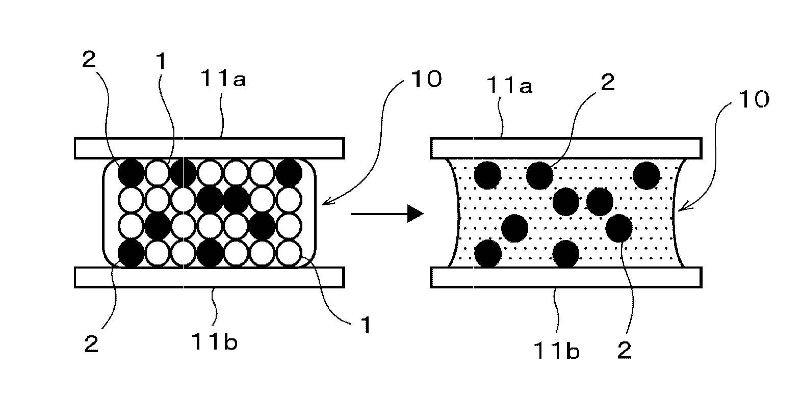
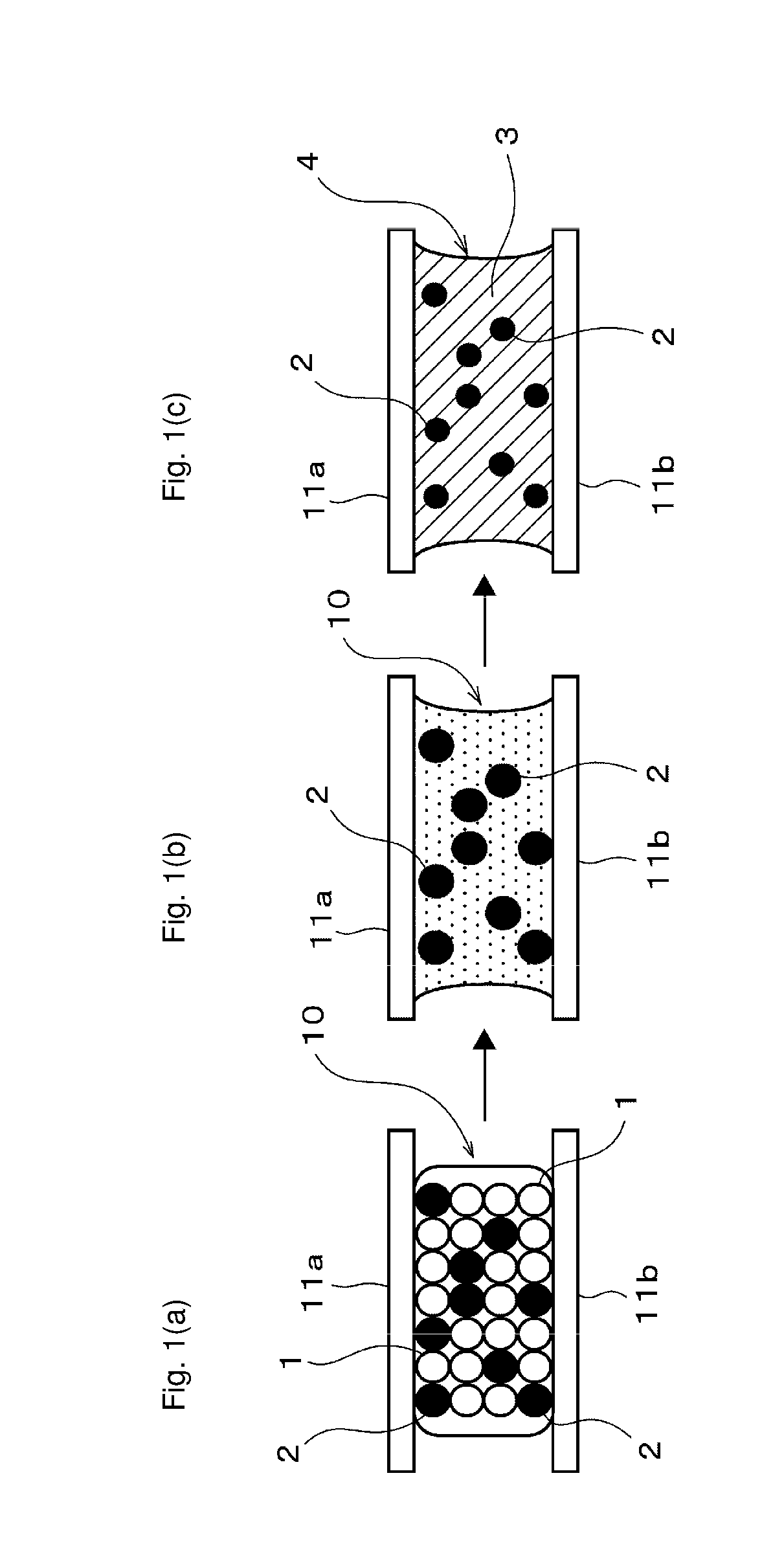
[0070]In this Example 1, a conductive material was prepared by mixing a powdered first metal (first metal powder), a powdered second metal (second metal powder) and a flux.

[0071]The compounding ratio of the first metal powder and the second metal powder was adjusted so that the volume ratio of the first metal powder / second metal powder was 60 / 40 (i.e. second metal: 40% by volume).

[0072]As the first metal powder, Sn-3Ag-0.5Cu, Sn, Sn-3.5Ag, Sn-0.75Cu, Sn-0.7Cu-0.05Ni, Sn-5Sb, Sn-2Ag-0.5Cu-2Bi, Sn-3.5Ag-0.5Bi-81n, Sn-9Zn, Sn-8Zn-3Bi, Sn-10Bi, Sn-15Bi, Sn-20Bi, Sn-30Bi, Sn-40Bi (Comparative Example), Sn-58Bi (Comparative Example) were used as shown in Table 1. The average particle size of the first metal powder was 25 μm.

[0073]Sn-40Bi and Sn-58Bi of the first metals described above are those of Comparative Examples which do not meet the requirement of the present invention that is “an alloy containing 70% by weight or more of Sn”.

[0074]In addition, Sn-3Ag-0.5Cu of the first metal was u...

example 2

[0105]A powder of Sn-3Ag-0.5Cu was prepared as the first metal powder. The average particle size of the first metal powder was 25 μm.

[0106]Powders of Cu-10Mn, Cu-10Ni and Cu (Comparative Example) were prepared as the second metal powder. The average particle size of the second metal powder was 15 μm.

[0107]As the flux, one having a compounding ratio of rosin: 74% by weight, diethylene glycol monobutyl ether: 22% by weight, triethanolamine: 2% by weight and hydrogenated castor oil: 2% by weight was prepared.

[0108]A conductive material was prepared by mixing the above-mentioned first metal powder, second metal powder and flux.

[0109]The compounding ratio of the first metal powder and the second metal powder was adjusted so that the volume ratio of the first metal powder / second metal powder was 87 / 13 to 57 / 43 (i.e. second metal powder: 13 to 43% by volume).

[0110]For the compounding ratio of the flux, the ratio of the flux to the entire conductive material was 10% by weight.

[0111]For the ...

example 3

[0119]A powder of Sn-3Ag-0.5Cu was prepared as the first metal powder. The average particle size of the first metal powder was 25 μm.

[0120]As the second metal powder, a powder of a Cu—Mn alloy with the ratio of Mn of 5 to 30% by weight and a powder of a Cu—Ni alloy with the ratio of Ni of 5 to 20% by weight were prepared, and a Cu powder was prepared as Comparative Example. The average particle size of the second metal powder was 15 μm.

[0121]As the flux, one having a compounding ratio of rosin: 74% by weight, diethylene glycol monobutyl ether: 22% by weight, triethanolamine: 2% by weight and hydrogenated castor oil: 2% by weight was prepared.

[0122]A conductive material was prepared by mixing the above-mentioned first metal powder, second metal powder and flux.

[0123]For the compounding ratio of the flux, the ratio of the flux to the entire conductive material was 10% by weight.

[0124]The compounding ratio of the first metal powder and the second metal powder was adjusted so that the v...


PUM

PropertyMeasurementUnit
melting pointaaaaaaaaaa
specific surface areaaaaaaaaaaa
melting pointaaaaaaaaaa

Abstract

A conductive material that includes a metal component consisting of a first metal and a second metal having a melting point higher than that of the first metal, wherein the first metal is Sn or an alloy containing 70% by weight or more of Sn, and the second metal is a metal or alloy which forms an intermetallic compound having a melting point of 310° C. or higher with the first metal and has a lattice constant difference of 50% or greater between itself and the intermetallic compound generated at the circumference of the second metal.

Description

CROSS REFERENCE TO RELATED APPLICATIONS[0001]The present application is a continuation of International application No. PCT / JP2011 / 054632, filed Mar. 1, 2011, which claims priority to Japanese Patent Application No. JP2010-259131, filed Nov. 19, 2010, the entire contents of each of which are incorporated herein by reference.FIELD OF THE INVENTION[0002]The present invention relates to a conductive material, a bonding method using the same, and a bonded structure, and particularly to a conductive material for use in mounting of an electronic component and via bonding, a bonding method using the same and a bonded structure.BACKGROUND OF THE INVENTION[0003]As a conductive material used for mounting electronic components, solder is widely used.[0004]For Sn—Pb-based solder which has been widely used, methods of bonding with temperature hierarchy are widely applied in which high-temperature solder, for example Pb rich Pb-5Sn (melting point: 314 to 310° C.) or Pb-10Sn (melting point: 302 to...

Claims


Application Information

Patent Timeline
Patent Type & Authority Applications(United States)
IPC IPC(8): H01R4/02B23K1/00B23K35/24B22F1/052B22F1/10B22F1/17
CPCC22C9/00C22C13/02H01R4/02B23K35/24B23K1/00B23K35/262B23K35/302B22F1/025C22C1/0483C22C1/0491B22F1/0059B22F7/064B22F7/08C22C9/05C22C9/06C22C13/00H01R4/04B23K35/025C22C9/02B22F1/052B22F1/17B22F1/10C22C1/047B23K35/22B23K35/26B23K35/30
Inventor NAKANO, KOSUKETAKAOKA, HIDEKIYO
Owner MURATA MFG CO LTD
Why Eureka
Try Eureka