Semiconductor device having buried gate, method of fabricating the same, and module and system having the same

a semiconductor device and buried gate technology, applied in semiconductor devices, digital storage, instruments, etc., can solve the problems of reducing the write-recovery time (twr), reducing the speed and current driving capability of the semiconductor device, and preventing the degraded device characteristics and reliability. , to achieve the effect of improving gidl, reducing resistance, and preventing the degrade of device characteristics and reliability

Active Publication Date: 2014-03-06
SK HYNIX INC
View PDF8 Cites 16 Cited by
  • Summary
  • Abstract
  • Description
  • Claims
  • Application Information

AI Technical Summary

Benefits of technology

[0009]Embodiments of the present invention may improve GIDL and prevent device characteristics and reliability from being degraded by reducing resistance in a buried gate. According to one aspect of an embodiment, a semiconductor device is provided. The semiconductor device may include: a semiconductor substrate having

Problems solved by technology

However, while over-etching the conductive material (gate electrode) of the buried gate can reduce leakage current, it also causes the speed and current dr

Method used


Image

  • Semiconductor device having buried gate, method of fabricating the same, and module and system having the same
  • Semiconductor device having buried gate, method of fabricating the same, and module and system having the same
  • Semiconductor device having buried gate, method of fabricating the same, and module and system having the same

Examples


first embodiment

[0033]FIGS. 3A to 3G are cross-sectional views illustrating a method of fabricating the semiconductor device according to the present invention;

second embodiment

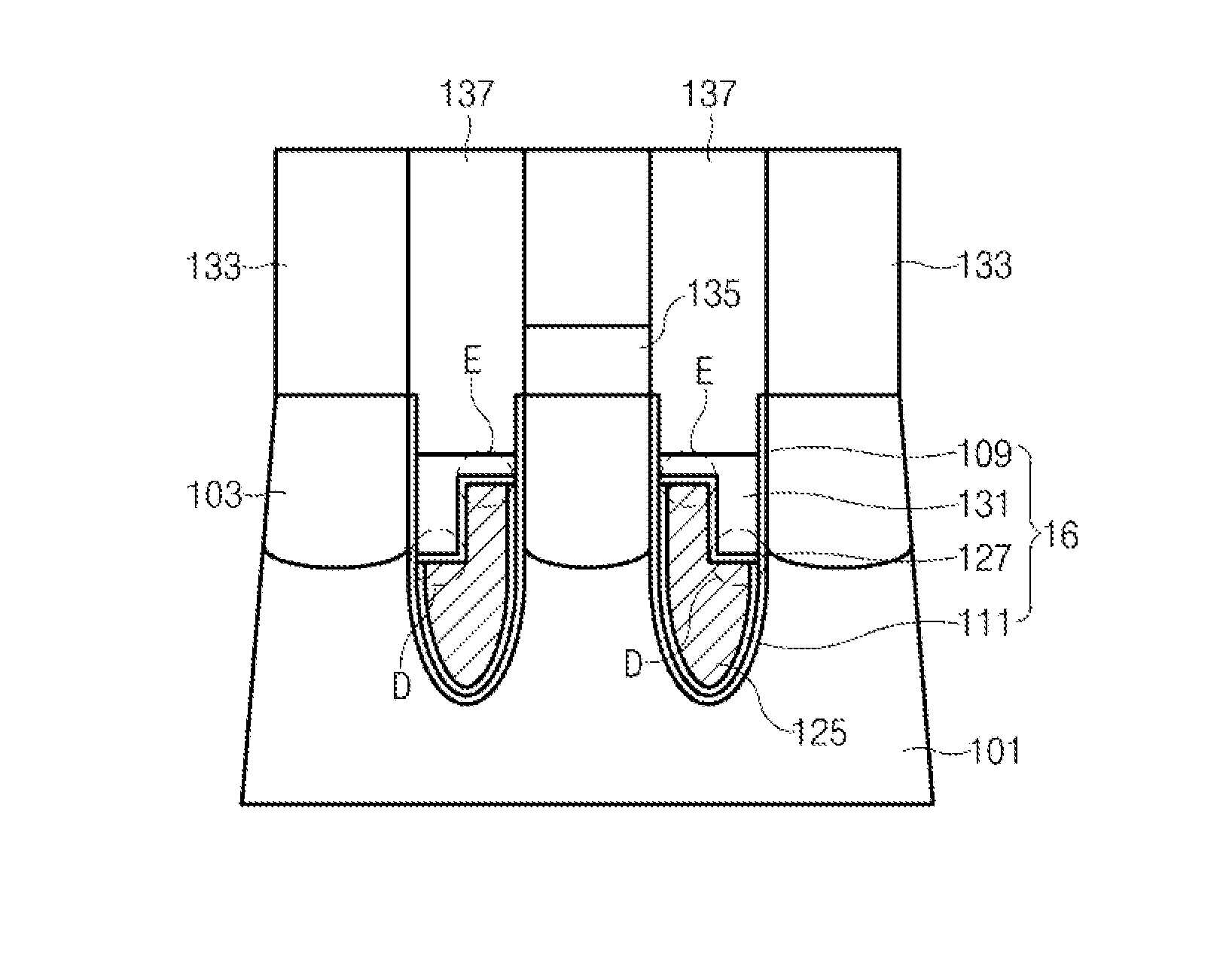
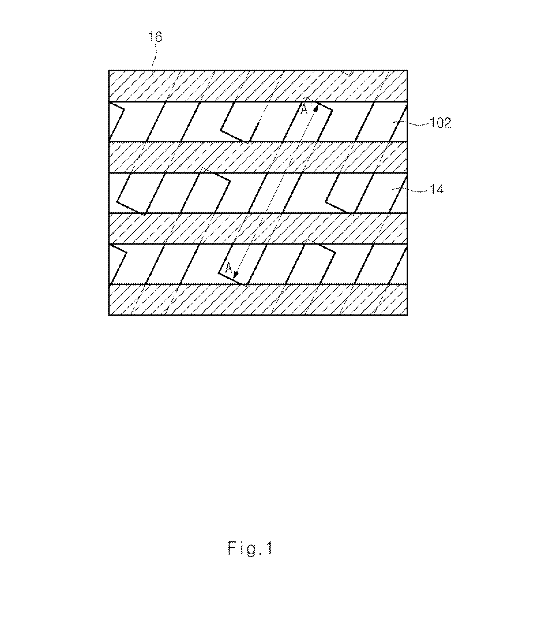
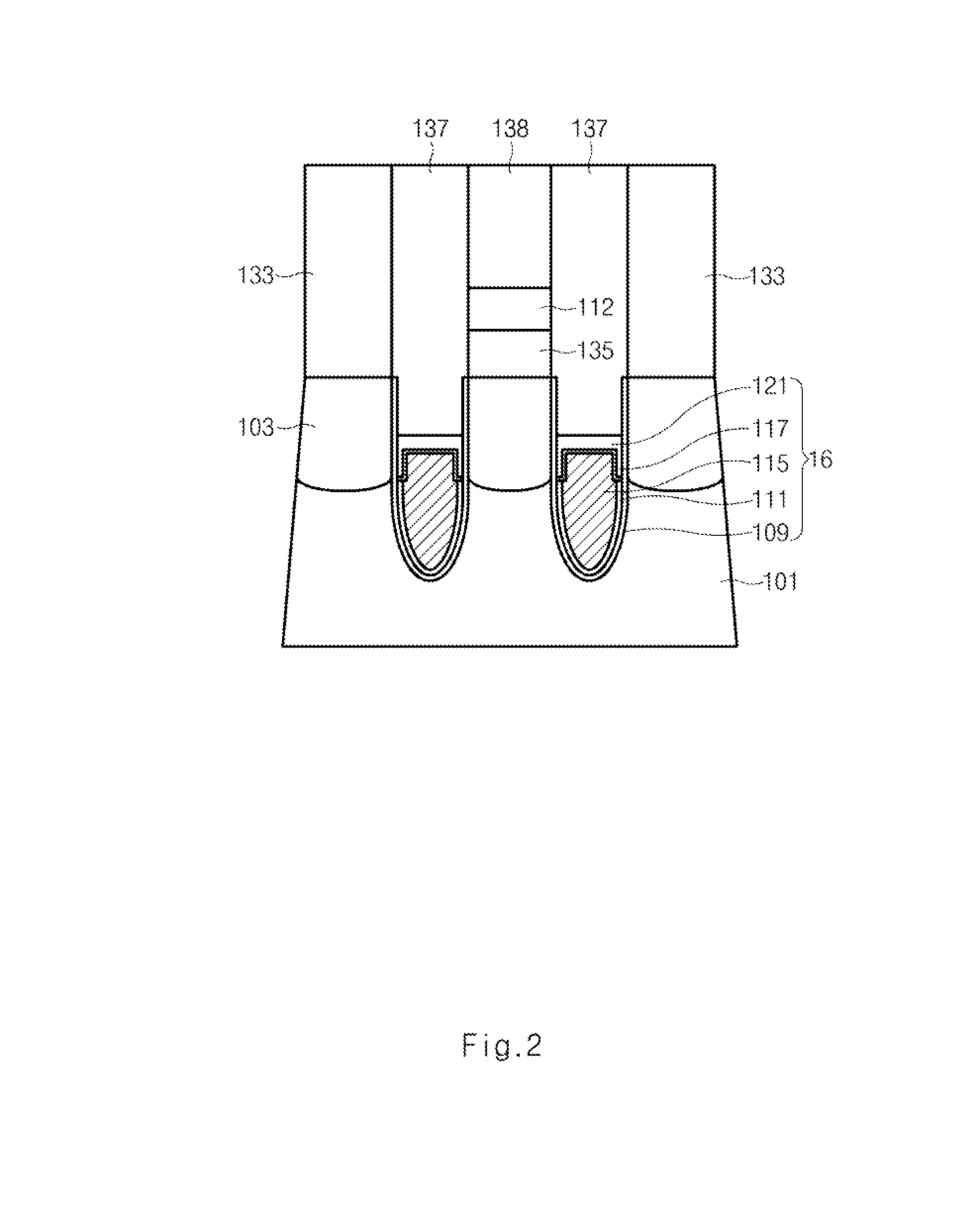
[0034]FIG. 4 is a cross-sectional view illustrating a semiconductor device taken along line A-A′ of FIG. 1 according to the present invention;

[0035]FIGS. 5A to 5G are cross-sectional views illustrating a method of fabricating the semiconductor device according to the second embodiment of the present invention;

[0036]FIG. 6 is a view illustrating a configuration in which a structure of a semiconductor device is expanded to a peripheral circuit area according to embodiments of the present invention;

[0037]FIG. 7 is a view illustrating a configuration of a semiconductor module according to embodiments of the present invention;

[0038]FIG. 8 is a view illustrating a configuration of a semiconductor system according to embodiments of the present invention;

[0039]FIG. 9 is a view illustrating a structure of a computer system according to embodiments of the present invention;

[0040]FIG. 10 is a view illustrating a configuration of a data processing system according to embodiments of the present ...


PUM


Abstract

A semiconductor device includes junction regions formed in upper portions of both sidewalls of a trench formed in a semiconductor substrate, a first gate electrode buried in the trench and having a stepped upper surface, and a second gate electrode formed on the first gate electrode to overlap a junction region.

Description

CROSS-REFERENCES TO RELATED APPLICATION[0001]This application claims priority under 35 U.S.C. 119(a) to Korean application number 10-2012-0096488, filed on 31 Aug. 2012, in the Korean Patent Office, which is incorporated by reference in its entirety.BACKGROUND OF THE INVENTION[0002]1. Technical Field[0003]The present invention relates to a buried gate type semiconductor device, a method of fabricating the same, and a module and system having the same, and more particularly, to technology related to improving gate-induced drain leakage (GIDL) and reducing a gate resistance, and thus improving device characteristics and reliability.[0004]2. Related Art[0005]Demand for higher capacity memory such as dynamic random access memories (DRAM) continues to increase while the size available for memory in many devices decreases or remains the same. Therefore, recent endeavors have focused on reducing a cell area by changing a cell layout to integrate more many memory cells on one wafer.[0006]Bu...

Claims


Application Information

Patent Timeline
IPC IPC(8): H01L29/78G11C11/4091H01L29/66
CPCH01L29/7827G11C11/4091H01L29/66666H01L29/945G11C11/404G11C2211/4068H01L29/4236G06F13/4068H10B12/34H10B12/0335H10B12/485H10B12/053H10B12/315H01L21/265H01L21/28035H01L21/28079H01L21/28088H01L21/30604H01L21/32133G11C11/4087
Inventor OH, TAE KYUNGYOO, MIN SOO
Owner SK HYNIX INC
Why Eureka
Try Eureka