

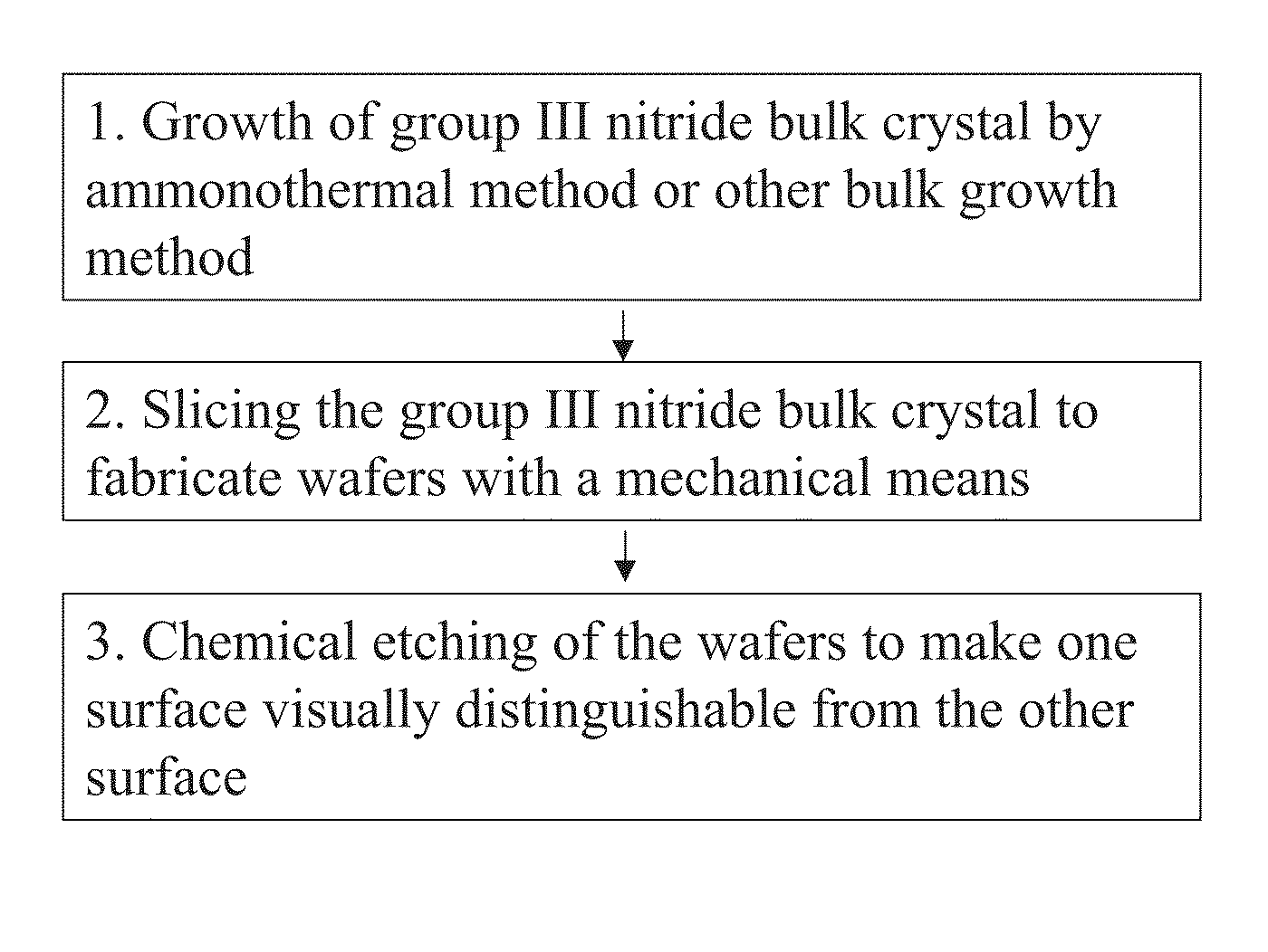
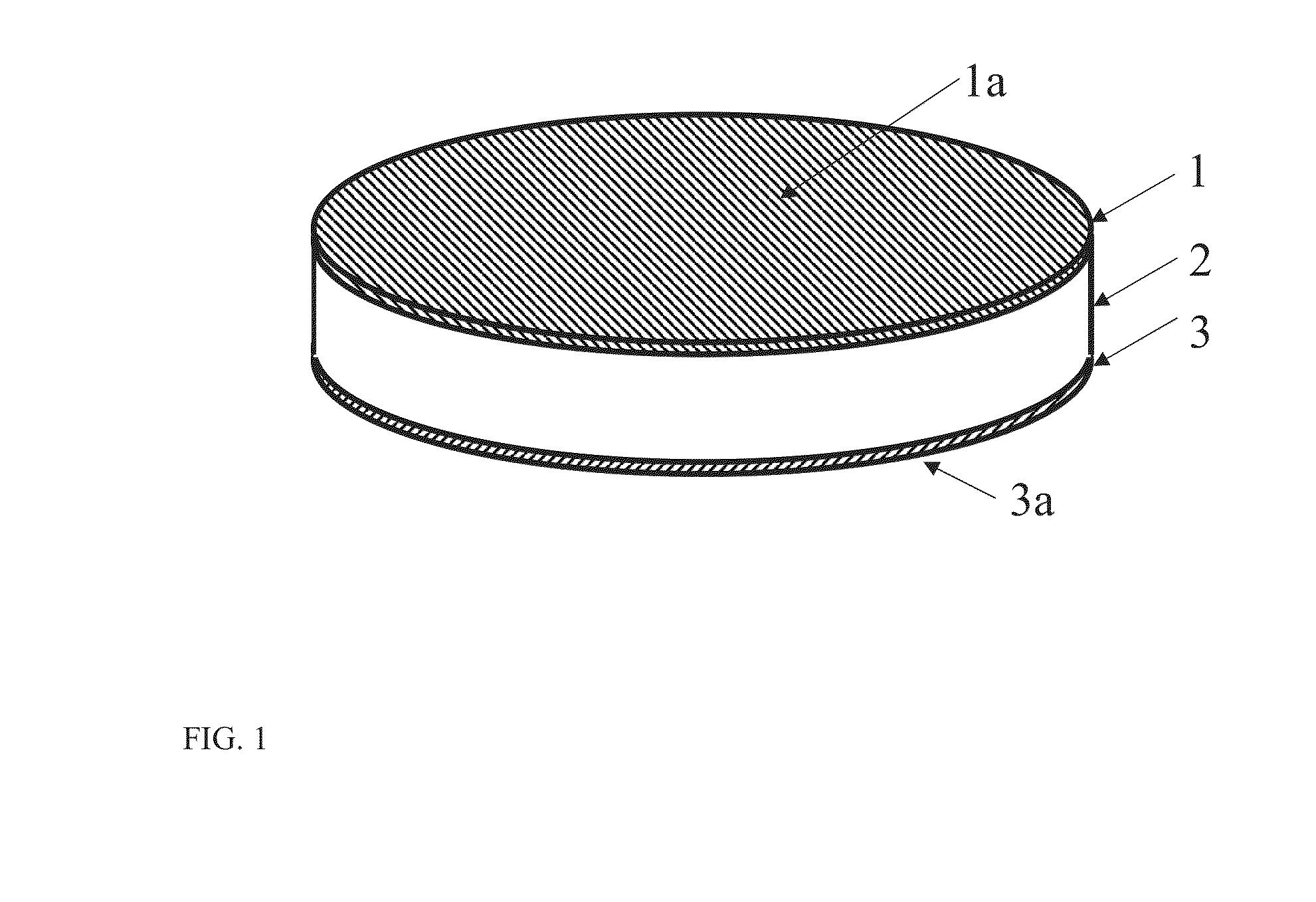
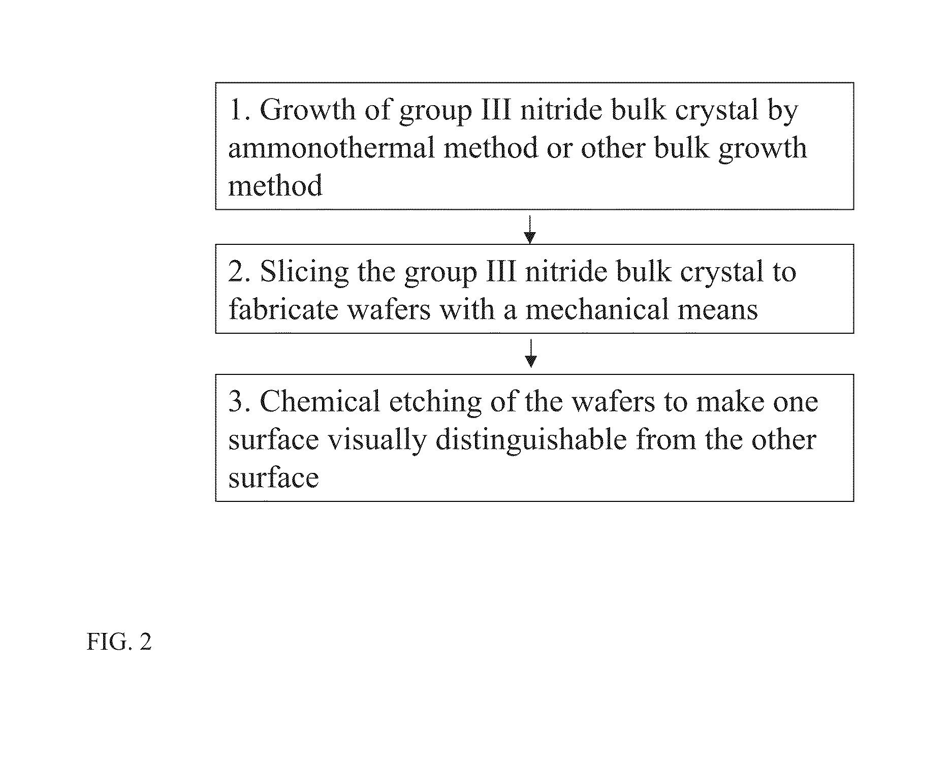
Group iii nitride wafer and its production method
a technology of nitride and nitride, which is applied in the field of group iii nitride wafer and its production method, can solve the problems of both surfaces of the wafer becoming rough
- Summary
- Abstract
- Description
- Claims
- Application Information
AI Technical Summary
Benefits of technology
Problems solved by technology
Method used
Image

Examples
example 1
[0039]Bulk crystal of GaN was grown on a GaN seed crystal with an ammonothermal method using polycrystalline GaN as a nutrient, supercritical ammonia as a solvent, and sodium (5 mol % to ammonia) as a mineralizer. The temperature was between 500 to 550 C and pressure was between 170 and 240 MPa. The thickness of the crystal was 6.9 mm and the surface area was approximately 100 mm2. A full-width half maximum (FWHM) of the X-ray diffraction from 002 plane was 900 arcsec. From this FWHM number, we estimate the density of line defects and grain boundaries is less than 106 cm−2. Although the crystal was not characterized with an optical and electrical measurement, those characteristics are expected to be the typical one for bulk crystal of GaN. For example, photoluminescence or cathode luminescence is expected to show luminescence from band-edge emission at around 370 nm, blue emission at around 400 nm, and / or yellow luminescence at around 600 nm. Conductivity type is expected to be n−ty...
PUM
| Property | Measurement | Unit |
|---|---|---|
| surface area | aaaaa | aaaaa |
| thickness | aaaaa | aaaaa |
| pressure | aaaaa | aaaaa |
Abstract
Description
Claims
Application Information