Production of a GaN bulk crystal substrate and a semiconductor device formed on a GaN bulk crystal substrate

a technology of gan bulk crystal and semiconductor device, which is applied in the direction of crystal growth process, transportation and packaging, and under a protective fluid, can solve the problems of difficult to construct a high-power laser diode based on the construction of fig. 1 and other problems, to achieve the effect of large optical power

Inactive Publication Date: 2007-07-31
SUMITOMO CHEM CO LTD +1
View PDF23 Cites 14 Cited by
  • Summary
  • Abstract
  • Description
  • Claims
  • Application Information

AI Technical Summary

Benefits of technology

[0027]According to the present invention, a high-quality GaN bulk crystal substrate is obtained with a process suitable for mass-production, by continuously supplying N so as to compensate for the depletion of N occurring in the system in which precipitation of a GaN single crystal takes place. By using the GaN bulk crystal substrate thus obtained, it is possible to fabricate an optical semiconductor device that produces an optical radiation of blue to ultraviolet wavelength with a large optical power. Further, the GaN bulk crystal substrate can be used as a substrate of an electron device such as HEMT.

Problems solved by technology

On the other hand, the laser diode of FIG. 1 cannot eliminate the defects completely, and there remain substantial defects particularly in correspondence to the part on the SiO2 mask 4 as represented in FIG. 2.
However, the defect-free region formed on the opening 4A has a lateral size of only several microns, and thus, it is difficult to construct a high-power laser diode based on the construction of FIG. 1.
When the laser diode of FIG. 1 is driven at a high power, the area of optical emission in the active region extends inevitably across the defects, and the laser diode is damaged as a result of optical absorption caused by the defects.
Further, the laser diode of FIG. 1 having such a construction has other various drawbacks associated with the defects in the semiconductor epitaxial layers, such as large threshold current, limited lifetime, and the like.
Further, the laser diode of FIG. 1 has a drawback, in view of the fact that the sapphire substrate is an insulating substrate, in that it is not possible to provide an electrode on the substrate.
In addition, the increased distance between the active layer 7 and the n-type electrode 12 causes the problem of increased resistance of the current path, while such an increased resistance of the current path deteriorates the high-speed response of the laser diode.
Further, the conventional laser diode of FIG. 1 suffers from the problem of poor quality of mirror surfaces defining the optical cavity.
Due to the fact that the sapphire single crystal constituting the substrate 1 belongs to hexagonal crystal system, formation of the optical cavity cannot be achieved by a simple cleaving process.
It has been therefore necessary to form the mirror surfaces, when fabricating the laser diode of FIG. 1 by conducting a dry etching process, while the mirror surface thus formed by a dry etching process has a poor quality.
This process, however, can only provide an extremely small crystal in the order of 1 cm in diameter at best.
Further the process of Porowski requires a specially built pressure-resistant apparatus and a long time is needed for loading or unloading a source material, or increasing or decreasing the pressure and temperature.
Thus, the process of this prior art would not be a realistic solution for mass-production of a GaN bulk crystal substrate.
On the other hand, the process of Yamane relies upon the initially confined N2 molecules in the atmosphere and the N atoms contained in the NaN3 flux for the source of N. Thus, when the reaction proceeds, the N2 molecules in the atmosphere or the N atoms in the Na—Ga melt are depleted with the precipitation of the GaN crystal, and there appears a limitation in growing a large bulk crystal of GaN.
Thus, the process of Yamane et al. op cit., while being successful in forming a GaN bulk crystal at a relatively low pressure and temperature, cannot be used for a mass production of a GaN substrate in the industrial base.

Method used


Image

  • Production of a GaN bulk crystal substrate and a semiconductor device formed on a GaN bulk crystal substrate
  • Production of a GaN bulk crystal substrate and a semiconductor device formed on a GaN bulk crystal substrate
  • Production of a GaN bulk crystal substrate and a semiconductor device formed on a GaN bulk crystal substrate

Examples


first embodiment

[First Embodiment]

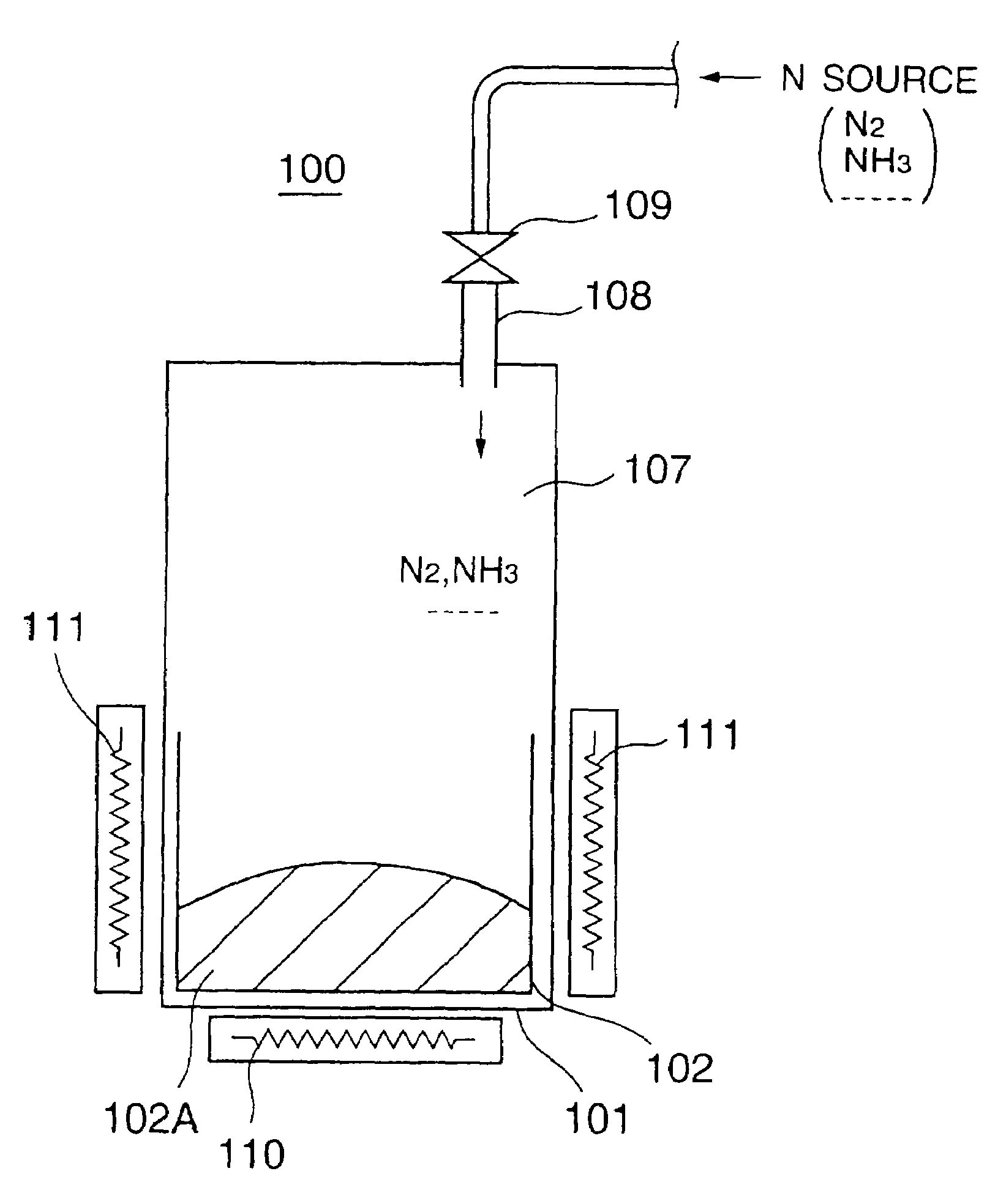
[0050]FIG. 3 shows the construction of a growth apparatus 100 used in a first embodiment of the present invention for growing a GaN bulk crystal.

[0051]Referring to FIG. 3, the growth apparatus 100 includes a pressure-resistant reaction vessel 101 typically of a stainless steel having an inner diameter of about 75 mm and a length of about 300 mm and accommodates therein a crucible 102 of Nb or BN. As will be explained later, the crucible 102 is loaded with a starting material of metallic Ga and a NaN3 flux and is confined in the reaction vessel 101 together with an N2 atmosphere 107. Further, the reaction vessel 101 is supplied with N2 or a gaseous compound of N from an external source via a regulator valve 109 and an inlet 108. The reaction vessel 101 thus loaded with the starting material in the crucible 102 is heated by energizing heaters 110 and 111 to a temperature of 650–850° C., and the pressure inside the reaction vessel is regulated to a moderate value of a...

second embodiment

[Second Embodiment]

[0063]FIG. 7 shows the construction of a growth apparatus 200 according to a second embodiment of the present invention, wherein those parts corresponding to the parts described previously are designated by the same reference numerals and the description there of will be omitted.

[0064]Referring to FIG. 7, the present embodiment uses heaters 111A and 111B in place of the heater 111 and induces a temperature gradient in the melt 102A for facilitating transport of Ga from the GaN fine crystals 102C or the GaNa intermetallic compound 102D to the melt surface.

[0065]More specifically, the heater 111B is provided in correspondence to the bottom part of the crucible 102 and controls, together with the heart 11A, the melt temperature at the bottom part of the crucible 102 lower than the melt surface. As a result of energization of the heaters 111A and 111B, a temperature gradient shown in FIG. 7 is induced.

[0066]Due to the increased temperature at the bottom part of the cr...

third embodiment

[Third Embodiment]

[0068]FIG. 8 shows the construction of a growth apparatus 300 according to a third embodiment of the present invention, wherein those parts corresponding to the parts described previously are designated by the same reference numerals and the description thereof will be omitted.

[0069]Referring to FIG. 8, the present embodiment is a modification of the embodiment of FIG. 7 and uses the heaters 110 and 111, described with reference to the growth apparatus 100 for inducing the desired temperature gradient. As other aspects of the present embodiment are substantially the same as those of the previous embodiment, further description will be omitted.


PUM

PropertyMeasurementUnit
thicknessaaaaaaaaaa
thicknessaaaaaaaaaa
temperatureaaaaaaaaaa

Abstract

A method of making a bulk crystal substrate of a GaN single crystal includes the steps of forming a molten flux of an alkali metal in a reaction vessel and causing a growth of a GaN single crystal from the molten flux, wherein the growth is continued while replenishing a compound containing N from a source outside the reaction vessel.

Description

[0001]This is a divisional of application Ser. No. 09 / 590,063 filed Jun. 8, 2000, now U.S. Pat. No. 6,592,663.BACKGROUND OF THE INVENTION[0002]The present invention generally relates to semiconductor devices and more particularly to a semiconductor device having a GaN bulk crystal substrate.[0003]GaN is a III-V compound semiconductor material having a large bandgap of blue to ultraviolet wavelength energy. Thus, intensive investigations are being made with regard to development of optical semiconductor devices having a GaN active layer for use particularly in optical information storage devices including a digital video data recorder (DVD). By using such a light emitting semiconductor device producing blue to ultraviolet wavelength optical radiation for the optical source, it is possible to increase the recording density of optical information storage devices.[0004]Conventionally, a laser diode or light-emitting diode having a GaN active layer has been constructed on a sapphire subs...

Claims


Application Information

Patent Timeline
Patent Type & Authority Patents(United States)
IPC IPC(8): H01L31/0328H01L31/0336H01L31/072H01L31/109C30B9/00C30B11/00C30B15/00
CPCC30B9/00C30B11/00C30B15/00C30B29/403C30B29/406H01L29/7783C30B7/00C09K11/62Y10T117/1092Y10T428/2982Y10T117/1096H01L29/2003C30B7/105
Inventor SARAYAMA, SEIJISHIMADA, MASAHIKOYAMANE, HISANORIIWATA, HIROKAZU
Owner SUMITOMO CHEM CO LTD
Why Eureka
Try Eureka