Manufacturing method for silicon carbide monocrystals

一种制造方法、单晶的技术,应用在化学仪器和方法、单晶生长、单晶生长等方向,能够解决难输出光、无法基板使用、降低载流子密度SiC单晶着色等问题,达到载流子密度低、着色少、高效载流子密度的效果

Inactive Publication Date: 2011-09-28
NIPPON STEEL CORP
View PDF2 Cites 15 Cited by
  • Summary
  • Abstract
  • Description
  • Claims
  • Application Information

AI Technical Summary

Problems solved by technology

Therefore, when using a SiC single crystal obtained by a solution growth method as a light-emitting element substrate, there is another disadvantage that it is difficult to output light from the back surface of the substrate by so-called flip-chip mounting, and it cannot be used as a substrate for lighting devices. use
This method is aimed at increasing the growth rate of SiC single crystals to make it possible to produce bulk single crystals (self-supporting crystals), and there is no description about reducing the carrier density and suppressing the coloring of SiC single crystals

Method used


Image

  • Manufacturing method for silicon carbide monocrystals
  • Manufacturing method for silicon carbide monocrystals
  • Manufacturing method for silicon carbide monocrystals

Examples


Embodiment

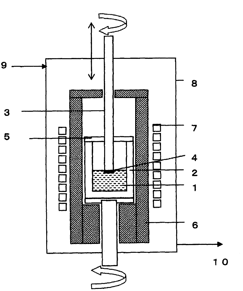
[0067] This example uses figure 1 In the shown single crystal manufacturing apparatus, a growth experiment of a SiC single crystal thin film was performed by the LPE method (temperature gradient method).

[0068] This single crystal manufacturing apparatus includes a high-purity graphite crucible 2 with an inner diameter of 80 mm and a height of 150 mm containing a SiC solution 1 in a molten state, and the crucible 2 is arranged in a water cooling chamber (stainless steel) 8 . The outer periphery of the graphite crucible is kept warm by a heat insulating material 6 , and a high frequency coil 7 for induction heating is provided on the outer periphery of the heat insulating material. The temperature distribution of the solution in the height direction can be controlled by adjusting the number of turns of the high-frequency coil, the pitch of the turns, and the relative positional relationship between the graphite crucible and the high-frequency coil. The atmosphere in the sin...


PUM

PropertyMeasurementUnit
carrier concentrationaaaaaaaaaa

Abstract

Disclosed is a method that can stably manufacture thin films or bulk crystals of SiC monocrystals that are suitable for use in various devices and have low carrier densities of 5 1017 / cm3 or less, and preferably less than 1 1017 / cm3, with liquid phase growth technology using a SiC solution that uses a molten Si alloy as the solvent. As the Si alloy, the method uses an alloy having a composition represented by SixCryTiz wherein x, y and z (each is atom%) satisfy (1) 0.50 < x < 0.68, 0.08 < y < 0.35 and 0.08 < z < 0.35 or (2) 0.40 < x = 0.50, 0.15 < y < 0.40 and 0.15 < z < 0.35. x, y and z preferably satisfy 0.53 < x < 0.65, 0.1 < y < 0.3 and 0.1 < z < 0.3.

Description

technical field [0001] The present invention relates to a method for manufacturing a silicon carbide (SiC) single crystal. The method of the invention can be applied to manufacture SiC single crystal substrates and wafers with SiC epitaxial films, which are especially suitable for electronic devices, optical devices and the like. Background technique [0002] Silicon carbide (SiC) has favorable material properties such as a wide band gap, high thermal conductivity, and low dielectric constant, so compared with silicon (Si) semiconductors, its operating loss is small, and semiconductor devices with high heat-resistant temperatures can be realized , It is expected to be used in a wide range of power device materials for power control, high-voltage high-frequency device materials, environment-resistant device materials used in high-temperature environments, and radiation-resistant device materials. [0003] No matter in which application, high-quality SiC single crystal is req...

Claims


Application Information

Patent Timeline
Patent Type & Authority Applications(China)
IPC IPC(8): C30B29/36C30B19/04
CPCC30B19/04C30B9/10C30B29/36C30B19/02C30B19/10H01L21/02
Inventor 龟井一人楠一彦矢代将齐八内昭博下崎新二
Owner NIPPON STEEL CORP
Why Eureka
Try Eureka