Semiconductor device

a technology of semiconductor devices and insulating components, applied in semiconductor devices, semiconductor/solid-state device details, electrical devices, etc., can solve the problems of unsatisfactory optical characteristics, foreign matter entering the hollow portion, and the hollow portion is not airtight, so as to achieve the effect of relieving vapor pressur

Active Publication Date: 2014-03-13
CANON KK
View PDF21 Cites 20 Cited by
  • Summary
  • Abstract
  • Description
  • Claims
  • Application Information

AI Technical Summary

Benefits of technology

[0008]Accordingly, an object of the present invention is to provide a semiconductor device which maintains airtightness of a hollow portion to prevent entry of foreign matters thereinto at ordinary temperature and which may relieve vapor pressure in the hollow portion when heated.
[0011]According to the present invention, the hollow portion is formed by being surrounded by the wiring substrate, the protective member, and the wall member. At ordinary temperature, the pillar member may maintain the airtightness of the hollow portion to prevent entry of foreign matters thereinto. When heated, water vapor in the hollow portion may be relieved to the outside through the vent hole at a place corresponding to the pillar member, thereby suppressing pressure rise in the hollow portion and preventing separation of the protective member.

Problems solved by technology

A semiconductor device having a hollow structure has a problem in that moisture which enters the hollow portion due to moisture absorption by an adhesive made from a resin or by a resin material of a wiring substrate or the like expands by reflow heating when the semiconductor device is mounted on a motherboard, and the vapor pressure of the moisture separates the protective member.
However, in the method described in PTL 1, the vent hole is always open even when the semiconductor device is not heated, and thus, there is a problem in that the hollow portion is not airtight and foreign matters enter the hollow portion.
Entry of foreign matters into the hollow portion has been a cause of a short circuit between electrically connected terminals.
Further, in a semiconductor device which uses an optical element as a semiconductor element, adhesion of foreign matters to a light receiving portion or a light emitting portion of the optical element has been a cause of unsatisfactory optical characteristics.

Method used


Image

  • Semiconductor device
  • Semiconductor device
  • Semiconductor device

Examples


first embodiment

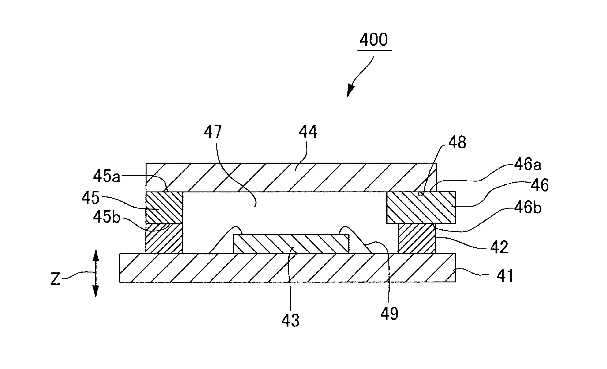
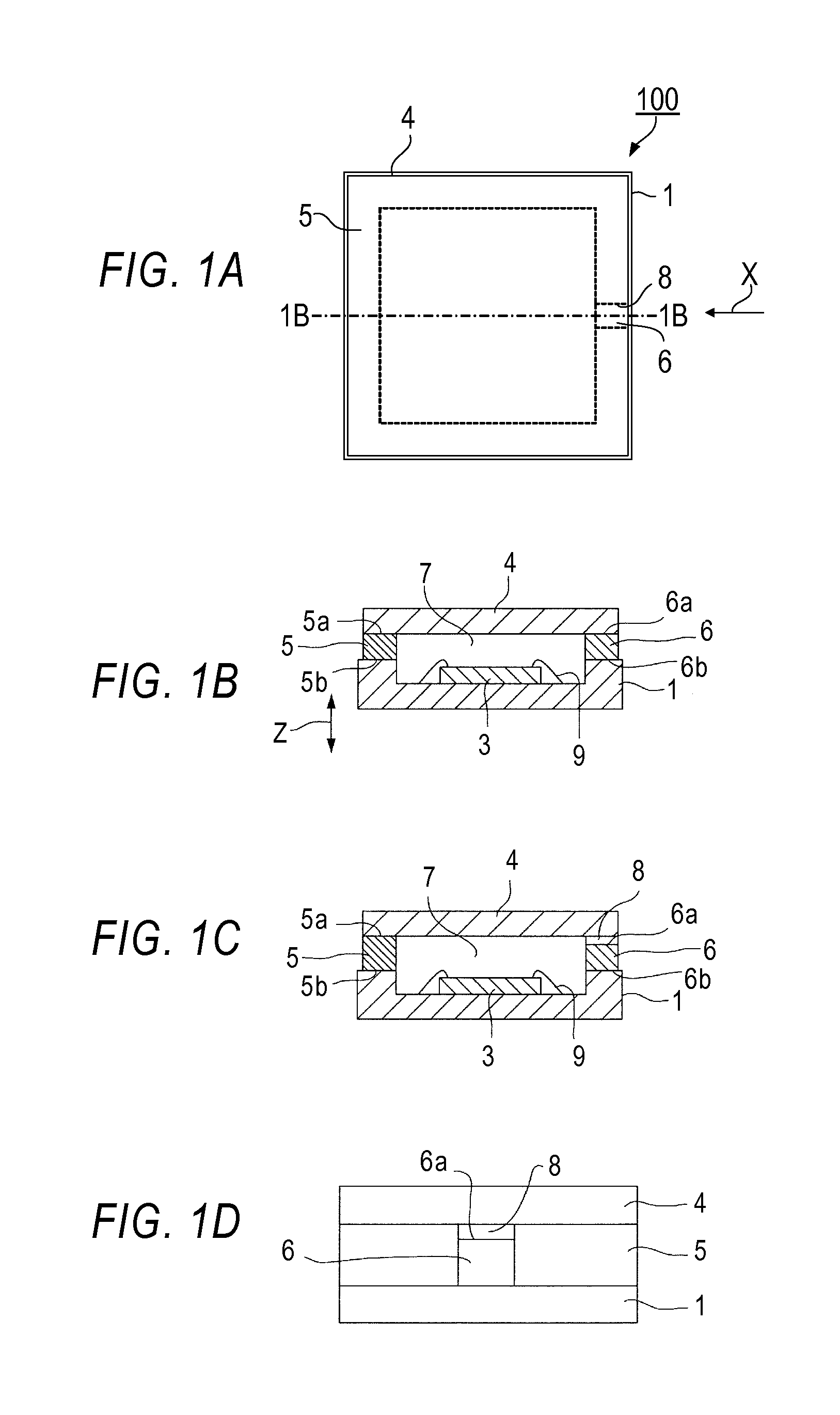
[0025]FIGS. 1A to 1D are explanatory views illustrating a schematic structure of a semiconductor device according to a first embodiment of the present invention. FIG. 1A is a plan view of the semiconductor device. FIG. 1B is a sectional view taken along the line 1B-1B of FIG. 1A of the semiconductor device in a state at ordinary temperature. FIG. 1C is a sectional view similar to FIG. 1B of the semiconductor device in a heated state. FIG. 1D is a side view illustrating a principal part of the semiconductor device in the heated state seen from the direction of an arrow X of FIG. 1A.

[0026]As illustrated in FIGS. 1A to 1D, a semiconductor device 100 includes a wiring substrate 1, a protective member 4 spaced from the wiring substrate 1, and a semiconductor element 3 placed between the wiring substrate 1 and the protective member 4 and electrically connected to the wiring substrate 1. The semiconductor element 3 is face-up mounted on the wiring substrate 1, and is electrically connected...

second embodiment

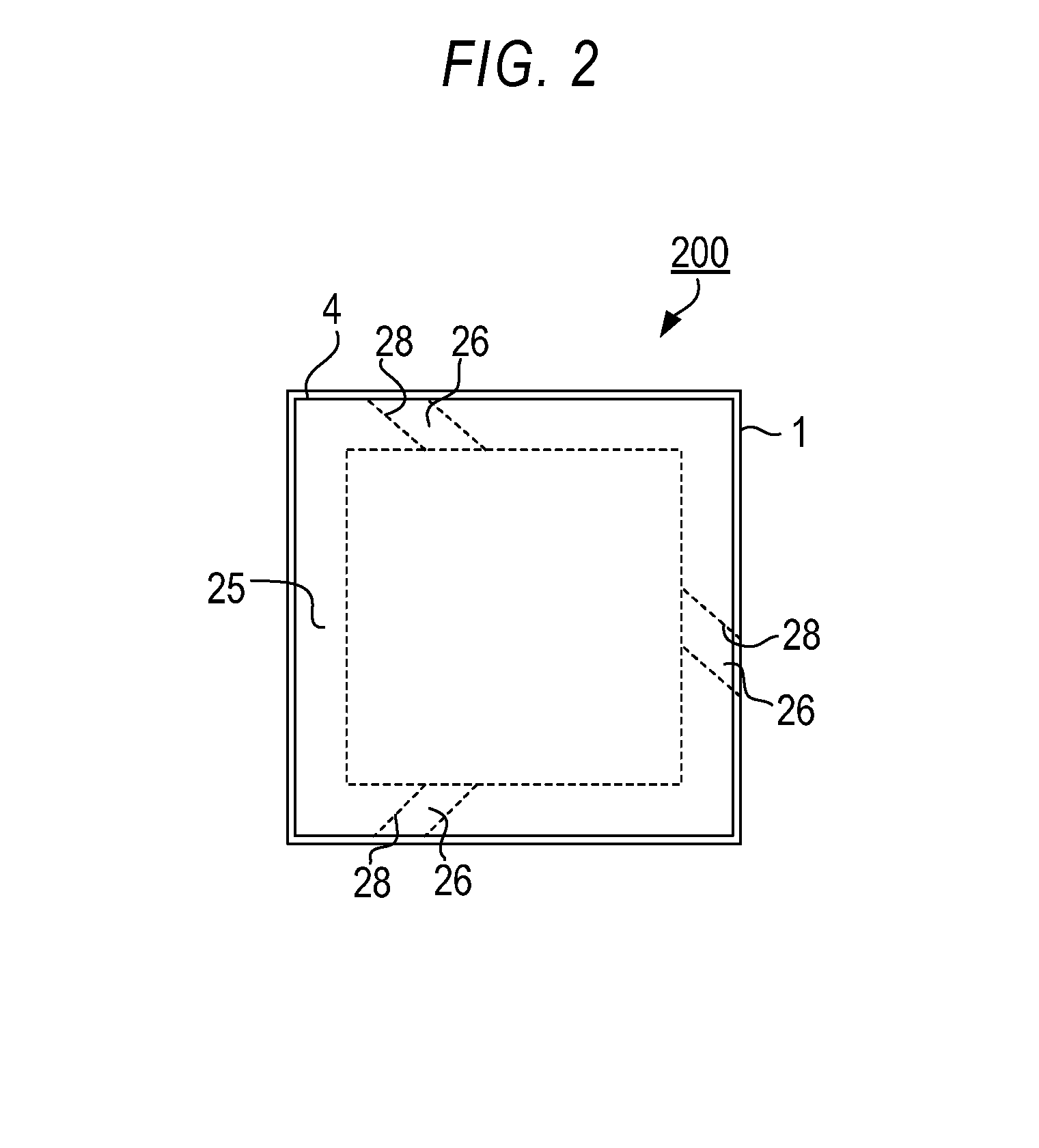
[0045]Next, a semiconductor device according to a second embodiment of the present invention is described. FIG. 2 is a plan view of the semiconductor device according to the second embodiment of the present invention.

[0046]In the second embodiment, similarly to the case of the above-mentioned first embodiment, a semiconductor device 200 includes a wall member 25, but the wall member 25 has multiple vent holes 28 provided therein. Each of the vent holes 28 is provided with a pillar member 26. In this case, during the course of the manufacturing process, when a liquid adhesive to be the wall member 25 after being cured is injected, the distance between the protective member 4 and the wiring substrate 1 may be accurately controlled through use of the pillar members 26 as spacers.

[0047]This causes the height of the wall member 25 existing between the wiring substrate 1 and the protective member 4 to be the same at various points in a peripheral direction, and a tilt of the protective me...

third embodiment

[0050]Next, a semiconductor device according to a third embodiment of the present invention is described. FIGS. 3A to 3C are explanatory views illustrating a schematic structure of the semiconductor device according to the third embodiment of the present invention. FIG. 3A is a plan view of the semiconductor device. FIG. 3B is a sectional view taken along the line 3B-3B of FIG. 3A of the semiconductor device in a state at ordinary temperature. FIG. 3C is a sectional view similar to FIG. 3B of the semiconductor device in a heated state.

[0051]As illustrated in FIGS. 3A to 3C, a semiconductor device 300 includes a wiring substrate 31 having an opening portion 31a formed therein and a protective member 34 spaced from the wiring substrate 31. Further, the semiconductor device 300 includes a semiconductor substrate 32 which is placed at a position opposed to the protective member 34 through the opening portion 31a of the wiring substrate 31 and which is electrically connected to the wirin...


PUM

PropertyMeasurementUnit
temperatureaaaaaaaaaa
thicknessaaaaaaaaaa
thicknessaaaaaaaaaa

Abstract

Provided is a semiconductor device in which a semiconductor element mounted on a wiring substrate is placed in a hollow portion, the hollow portion being formed by the wiring substrate, a protective member, and a wall member, with the wiring substrate, the protective member, and the wall member being a bottom surface, a top surface, and side surfaces thereof, respectively. The wall member has a vent hole provided therein, which communicates the hollow portion to / from the outside, and the vent hole includes a pillar member formed of a material having a linear expansion coefficient which is smaller than that of the wall member. Therefore, airtightness of the hollow portion is maintained to prevent entry of foreign matters at ordinary temperature, and vapor pressure in the hollow portion is relieved when heated.

Description

TECHNICAL FIELD[0001]The present invention relates to a semiconductor device having a hollow structure.BACKGROUND ART[0002]An image sensor package using a CCD image sensor or a CMOS image sensor used in a digital camera or a video camera, and a SAW filter package used in a cellular phone or the like are semiconductor devices having a hollow structure. A semiconductor device having a hollow structure has a structure in which, after a semiconductor element is mounted on a wiring substrate and electrodes of the semiconductor element and electrodes of the wiring substrate are electrically connected to each other through use of metal wires, a protective member is attached from above the wiring substrate so as to encapsulate the semiconductor element in a hollow portion.[0003]A semiconductor device having a hollow structure has a problem in that moisture which enters the hollow portion due to moisture absorption by an adhesive made from a resin or by a resin material of a wiring substrate...

Claims


Application Information

Patent Timeline
Patent Type & Authority Applications(United States)
IPC IPC(8): H01L23/52H01L23/498
CPCH01L23/49811H01L23/52H01L21/50H01L23/10H01L23/564H01L27/14618H01L31/0203H01L2924/09701H01L2224/48091H01L2924/00014
Inventor OKADA, YUYA
Owner CANON KK
Why Eureka
Try Eureka