
Tunable composite interposer

Active Publication Date: 2014-03-13
INVENSAS CORP
View PDF3 Cites 82 Cited by
  • Summary
  • Abstract
  • Description
  • Claims
  • Application Information

AI Technical Summary

Benefits of technology

This patent is about a support element that can be used in a composite interposer. The support element can be made of a mesophase material or liquid crystal material, and it can have a compliant dielectric layer along its surface. The terminals on the interposer can make contact with the compliant dielectric layer, and conductive vias can also be used to connect to the terminals. These conductive vias help to reduce stresses on the interposer caused by changes in temperature. The technical effect is that this design makes the interposer more robust and reliable for use in electronic components.

Problems solved by technology

Such a reduction in the available space on the first face that can be used for active circuitry may increase the amount of silicon required to produce each semiconductor chip, thereby potentially increasing the cost of each chip.
Conventional vias may have reliability challenges because of a non-optimal stress distribution radiating from the vias and a mismatch of the coefficient of thermal expansion (CTE) between a semiconductor chip, for example, and the structure to which the chip is bonded.
For example, when conductive vias within a semiconductor chip are insulated by a relatively thin and stiff dielectric material, significant stresses may be present within the vias due to CTE mismatch between the conductive material of the via and the material of the substrate.
In addition, when the semiconductor chip is bonded to conductive elements of a polymeric substrate, the electrical connections between the chip and the higher CTE structure of the substrate will be under stress due to CTE mismatch.

Method used


Image

  • Tunable composite interposer
  • Tunable composite interposer
  • Tunable composite interposer

Examples


Embodiment Construction

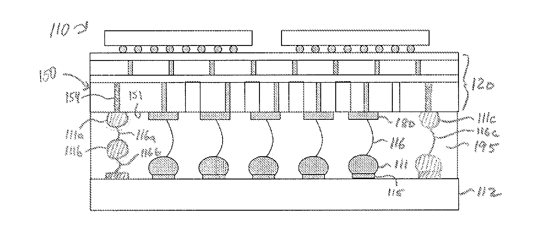
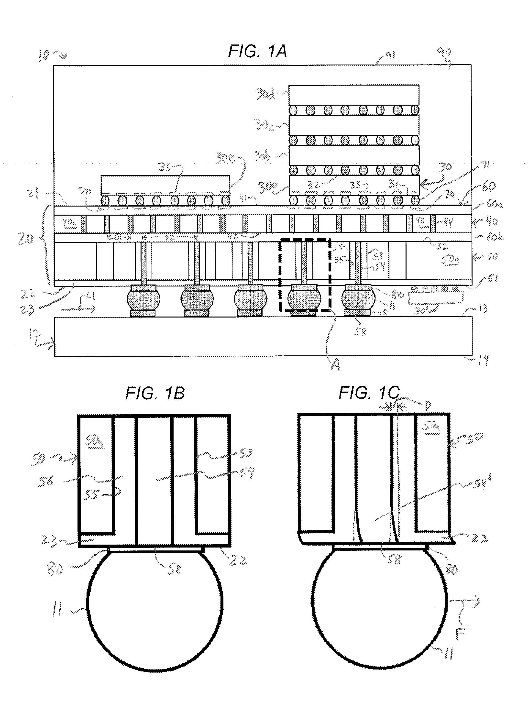
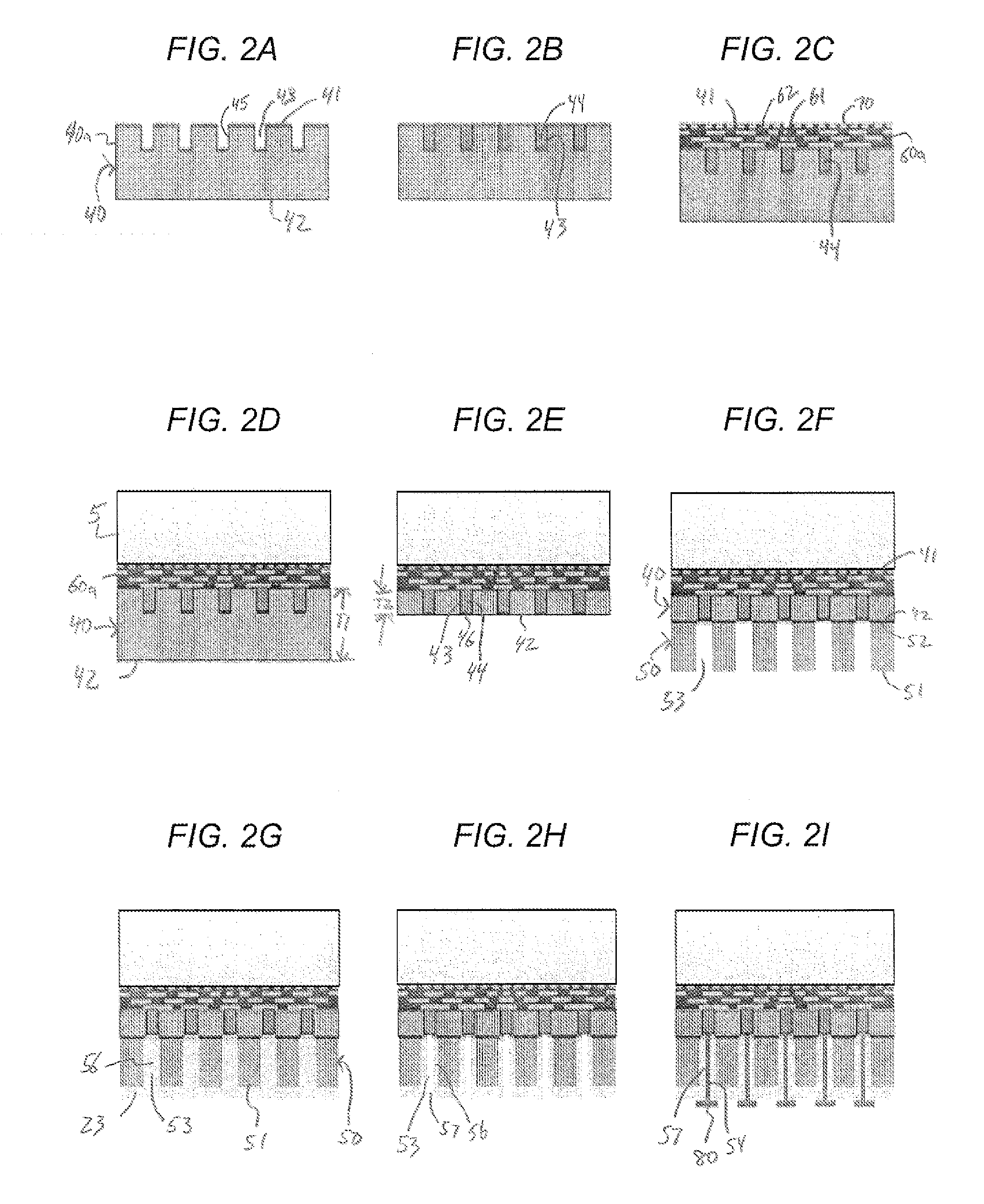
[0048]As illustrated in FIG. 1A, a microelectronic assembly 10 can include an interconnection element 20 having a first surface 21 and a second surface 22 opposite therefrom, one or more microelectronic elements 30 assembled with the interconnection element, an encapsulant 90 at least partially covering the microelectronic elements 30, and a circuit panel 12 assembled with the interconnection element.

[0049]In FIG. 1A, the directions parallel to the first surface 21 are referred to herein as “horizontal” or “lateral” directions, whereas the directions perpendicular to the first surface are referred to herein as upward or downward directions and are also referred to herein as the “vertical” directions. The directions referred to herein are in the frame of reference of the structures referred to. Thus, these directions may lie at any orientation to the normal or gravitational frame of reference. A statement that one feature is disposed at a greater height “above a surface” than another...


PUM


Abstract

A composite interposer can include a substrate element and a support element. The substrate element can have first and second opposite surfaces defining a thickness of 200 microns or less, and can have a plurality of contacts exposed at the first surface and electrically conductive structure extending through the thickness. The support element can have a body of at least one of dielectric or semiconductor material exposed at a second surface of the support element, openings extending through a thickness of the body, conductive vias extending within at least some of the openings in a direction of the thickness of the body, and terminals exposed at a first surface of the support element. The second surface of the support element can be united with the second surface of the substrate element. The terminals can be electrically connected with the contacts through the conductive vias and the electrically conductive structure.

Description

BACKGROUND OF THE INVENTION[0001]The present invention relates to packaging of microelectronic devices and interposer structures, especially conductive via structures and methods of forming such via structures in semiconductor and interposer packages.[0002]Microelectronic elements generally comprise a thin slab of a semiconductor material, such as silicon or gallium arsenide, commonly called a die or a semiconductor chip. Semiconductor chips are commonly provided as individual, prepackaged units. In some unit designs, the semiconductor chip is mounted to a substrate or chip carrier, which is in turn mounted on a circuit panel, such as a printed circuit board.[0003]The active circuitry is fabricated in a first face of the semiconductor chip (e.g., a second surface). To facilitate electrical connection to the active circuitry, the chip is provided with bond pads on the same face. The bond pads are typically placed in a regular array either around the edges of the die or, for many memo...

Claims


Application Information

Patent Timeline
IPC IPC(8): H01L23/48H01L23/00H01L21/768
CPCH01L23/481H01L24/03H01L21/76898H01L23/49822H01L23/49827H01L23/49833H01L23/4334H01L2224/131H01L2224/16145H01L2224/16225H01L2224/48227H01L2224/73253H01L2225/06517H01L2225/06589H01L2924/15311H01L2924/1815H01L2924/18161H01L2924/19106H01L2225/06513H01L24/13H01L24/14H01L24/16H01L24/48H01L24/73H01L25/0652H01L25/167H01L25/18H01L2224/14181H01L2924/1431H01L2924/1434H01L2924/157H01L2924/19105H01L2924/12041H01L2924/3011H01L2924/01322H01L2924/181H01L2924/12042H01L2224/0401H01L2924/00014H01L2924/014H01L2924/00H01L2924/00012H01L2224/45099H01L2224/45015H01L2924/207H01L21/4857H01L21/486H01L23/562
Inventor WOYCHIK, CHARLES G.UZOH, CYPRIAN EMEKASATO, HIROAKI
Owner INVENSAS CORP
Features
  • Generate Ideas
  • Intellectual Property
  • Life Sciences
  • Materials
  • Tech Scout
  • Unparalleled Data Quality
  • Higher Quality Content
  • 60% Fewer Hallucinations
Learn More