Wiring substrate and method for producing the same

a technology of wiring substrate and substrate, which is applied in the direction of resist details, mechanical equipment, machines/engines, etc., can solve the problems of difficulty in implementing a finer pitch disposition of connection terminals, and document 1 does not disclose the volume of the connection terminal portion

Inactive Publication Date: 2014-04-10
NGK SPARK PLUG CO LTD
View PDF5 Cites 21 Cited by
  • Summary
  • Abstract
  • Description
  • Claims
  • Application Information

AI Technical Summary

Benefits of technology

[0021]As described above, the present invention can provide a wiring substrate configured to implement

Problems solved by technology

However, Document 1 does not disclose the volume of the connection terminal portion that is exposed from the insulati

Method used


Image

  • Wiring substrate and method for producing the same
  • Wiring substrate and method for producing the same
  • Wiring substrate and method for producing the same

Examples


first embodiment

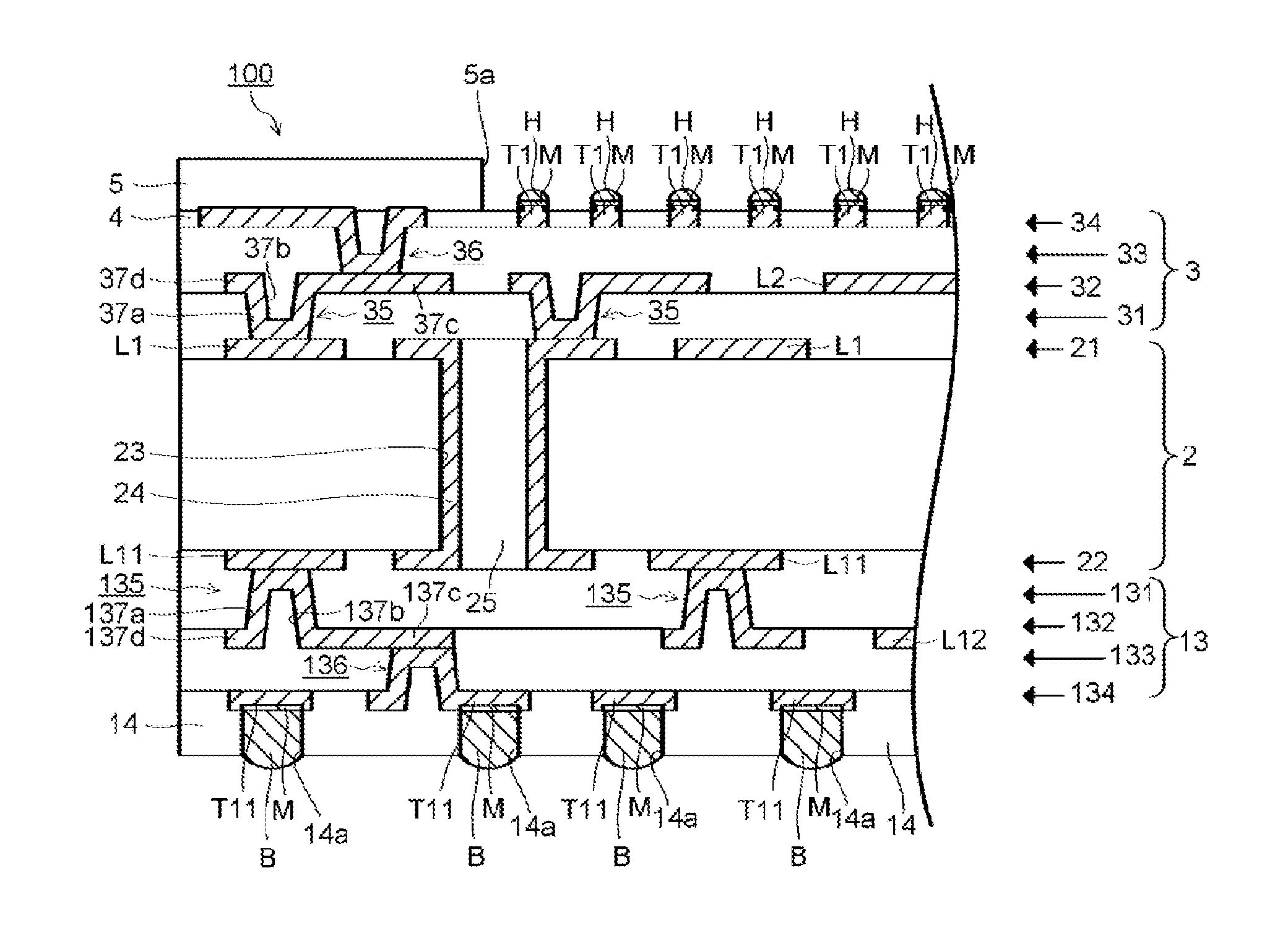
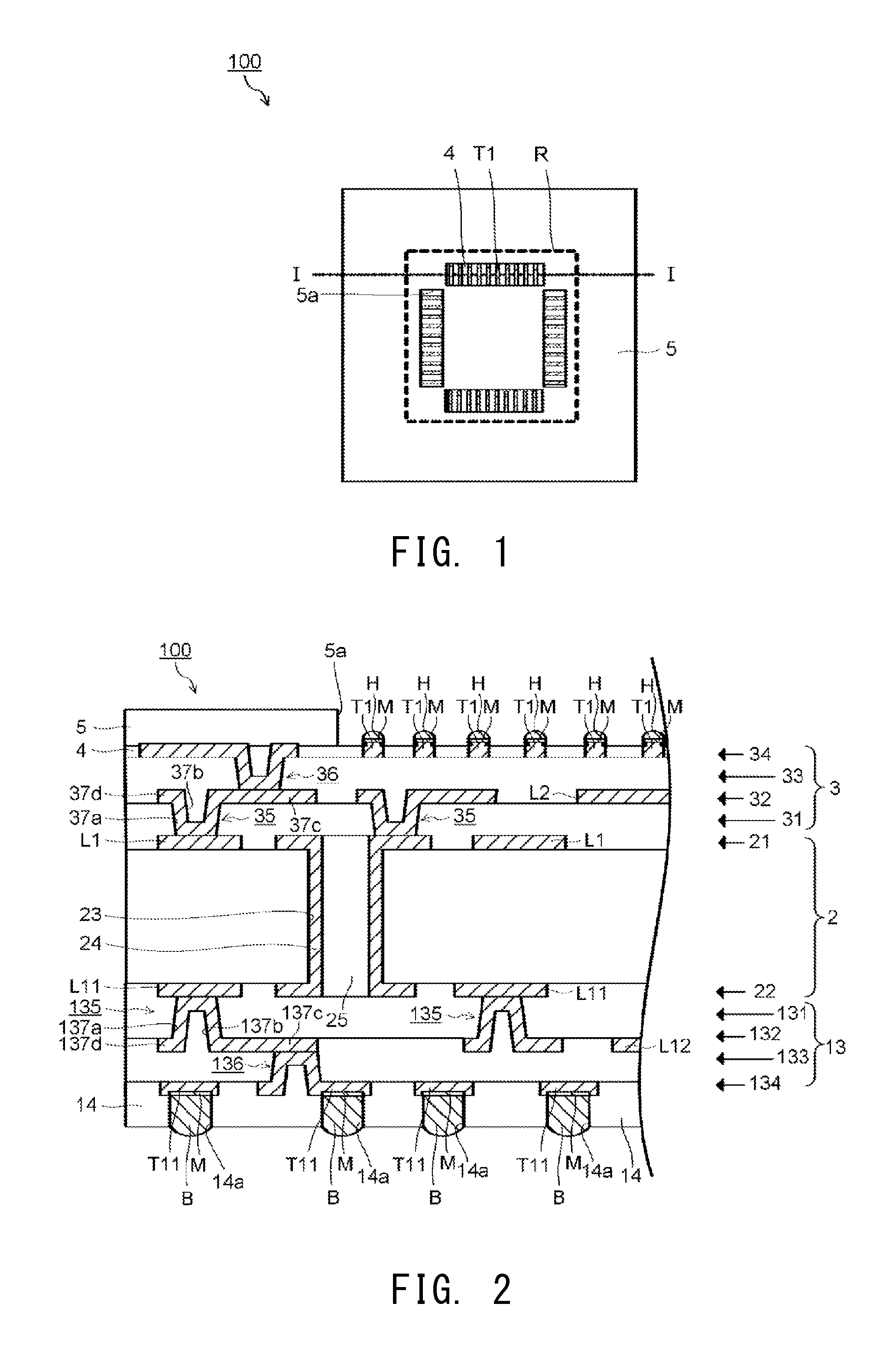
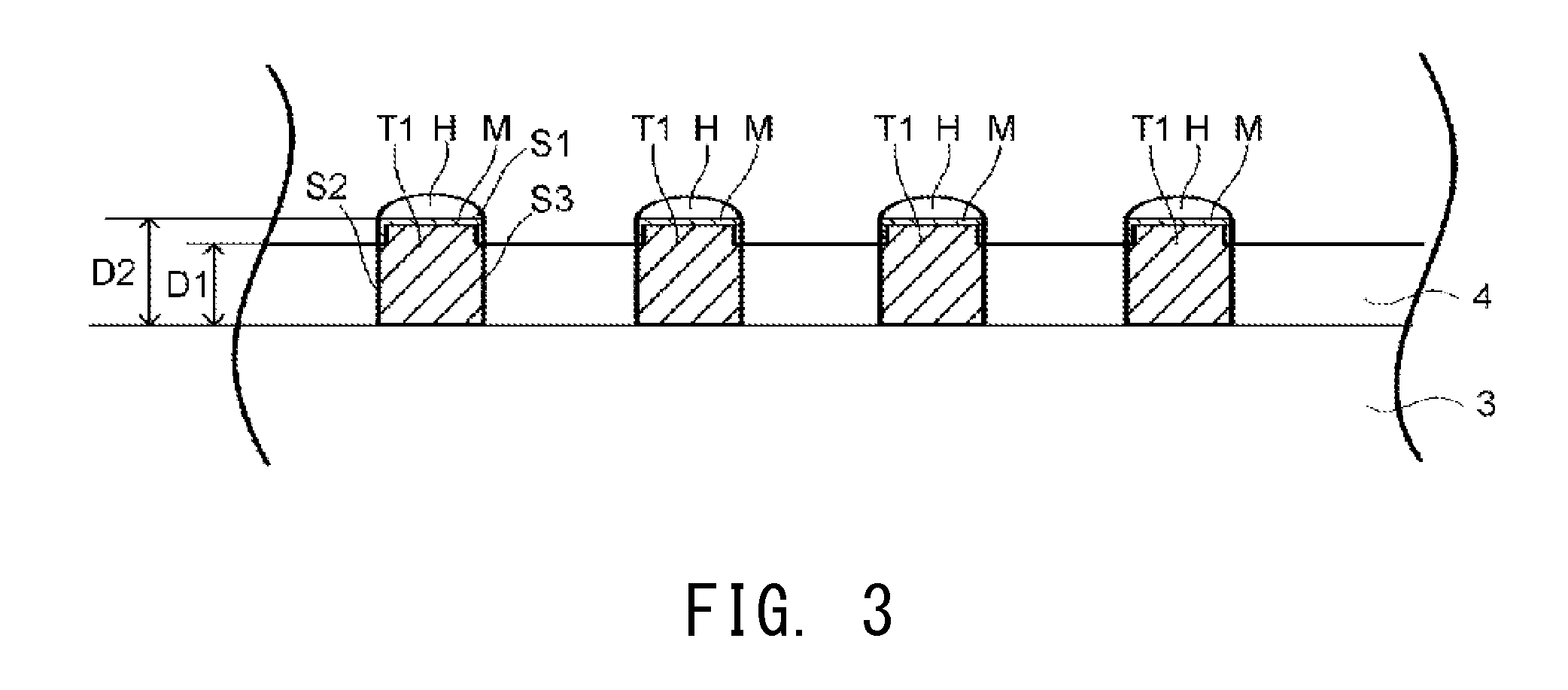
[0036]FIG. 1 is a plan view (front side) of a wiring substrate 100 according to a first embodiment. FIG. 2 is a fragmentary, sectional view of the wiring substrate 100 taken along line I-I of FIG. 1. FIG. 3 is an enlarged sectional view of connection terminals T1 formed on the front side of the wiring substrate 100. In the following description, a surface side of the wiring substrate 100 on which a semiconductor chip is connected is referred to as the front surface side (upper surface side), and a surface side on which a motherboard, a socket, or the like (hereinafter, referred to as a motherboard or the like) is connected is referred to as the back surface side (lower surface side).

Configuration of the Wiring Substrate 100

[0037]The wiring substrate 100 shown in FIGS. 1 to 3 includes a core substrate 2; a build-up layer 3 (front side) on which a plurality of the connection terminals T1 are formed for connection to a semiconductor chip (not shown) and which is stacked on the front si...

examples

[0072]The present invention will next be described in more detail by way of examples, which should not be construed as limiting the invention thereto. The present inventors produced connection terminals each having a top surface whose area is larger than that of each of opposite side surfaces thereof (Example) and connection terminals each having a top surface whose area is smaller than that of each of opposite side surfaces thereof (Comparative Example). Each connection terminal was plated with tin (Sn) through electroless plating, and the tin (Sn) plating was melted by heating. Photographs (enlarged) cross sections of the connection terminals are shown in FIGS. 12(a) and 12(b).

[0073]FIG. 12(a) is a photographic image of the connection terminal of the Example, and FIG. 12(b) is a photographic image of the connection terminal of the Comparative Example. As is clear from FIG. 12(a), tin (Sn) was present preferentially on the top surface of the connection terminal of Example to form a...


PUM


Abstract

Embodiments of the present wiring substrate include a stacked body including one or more insulation layers and one or more conductive layers, wherein the wiring substrate has a plurality of connection terminals formed on the stacked body, each connection terminal has a top surface whose area is smaller than that of each of opposite side surfaces thereof, and a filling member provided in a filling manner between the connection terminals. The top surface of each connection terminal has an area larger than that of a portion of each side surfaces portion exposed from the filling member, and a bonding layer containing a solder is formed on the top surface.

Description

CROSS REFERENCE TO RELATED APPLICATIONS[0001]The present application claims priority from Japanese Patent Application No. 2012-224025, which was filed on Oct. 9, 2012, the disclosure of which is herein incorporated by reference in its entirety.BACKGROUND OF THE INVENTION[0002]1. Field of the Invention[0003]The present invention relates to a wiring substrate having a plurality of connection terminals formed on its main surface for connection to a semiconductor chip, and to a method for producing the wiring substrate.[0004]2. Description of Related Art[0005]Usually, a wiring substrate has terminals formed on its main surface (front surface) for connection to a semiconductor chip (hereinafter referred to as connection terminals). In recent years, the disposition density of the connection terminals has been increasing; accordingly, the pitch between the connection terminals to be disposed has become finer. Thus, there is proposed a wiring substrate which employs the NSMD (non solder mas...

Claims


Application Information

Patent Timeline
IPC IPC(8): H05K1/02H05K3/00
CPCH05K3/00H05K1/0265H05K3/3452H05K3/4007H05K2201/09881H05K2203/0574H05K3/3485
Inventor NAGAI, MAKOTOMORI, SEIJIHAYASHI, TAKAHIROITO, TATSUYA
Owner NGK SPARK PLUG CO LTD
Why Eureka
Try Eureka