
Solar cell with reduced absorber thickness and reduced back surface recombination

a solar cell and absorber technology, applied in the field of thin film solar cells, can solve problems such as the reduction of the efficiency of the solar cell

Inactive Publication Date: 2014-04-17
IBM CORP
View PDF18 Cites 10 Cited by
  • Summary
  • Abstract
  • Description
  • Claims
  • Application Information

AI Technical Summary

Benefits of technology

This patent describes a thin-film solar cell and its manufacturing process. The cell consists of a substrate, reflecting material, dielectric, semiconducting material, and transparent layers. The manufacturing process involves depositing layers of the different materials on the substrate and then etching to create the desired pattern. The resulting solar cell has improved performance and efficiency. Additionally, this patent also describes a method for manufacturing a stacked-layered solar cell, which involves depositing layers of the different materials on a substrate and then etching to create the desired pattern. This manufacturing process allows for the creation of a more complex solar cell with improved performance.

Problems solved by technology

Shortcomings however, include the back contact of a solar cell having reduced reflectance for infrared wavelengths and a surface with a high probability for charge carrier recombination leading to decreased efficiency of the solar cell.

Method used


Image

  • Solar cell with reduced absorber thickness and reduced back surface recombination
  • Solar cell with reduced absorber thickness and reduced back surface recombination
  • Solar cell with reduced absorber thickness and reduced back surface recombination

Examples


Embodiment Construction

[0013]It will be readily understood that the components of the present invention, as generally described and illustrated in the Figures herein, may be arranged and designed in a wide variety of different configurations. Thus, the following detailed description of the embodiments of the apparatus, system, and method of the present invention, as presented in the Figures, is not intended to limit the scope of the invention, as claimed, but is merely representative of selected embodiments of the invention.

[0014]Reference throughout this specification to “a select embodiment,”“one embodiment,” or “an embodiment” means that a particular feature, structure, or characteristic described in connection with the embodiment is included in at least one embodiment of the present invention. Thus, appearances of the phrases “a select embodiment,”“in one embodiment,” or “in an embodiment” in various places throughout this specification are not necessarily referring to the same embodiment.

[0015]Furthe...


PUM


Abstract

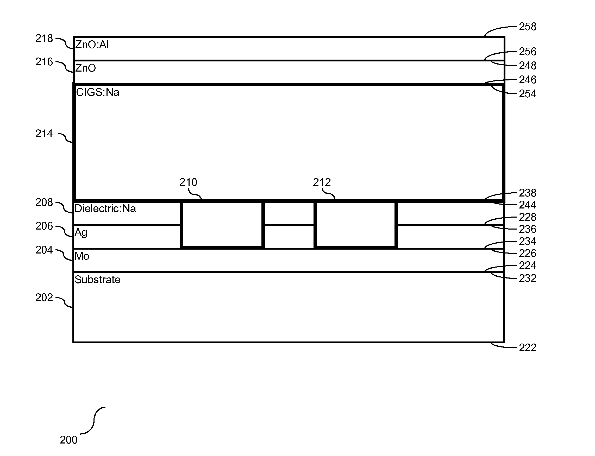
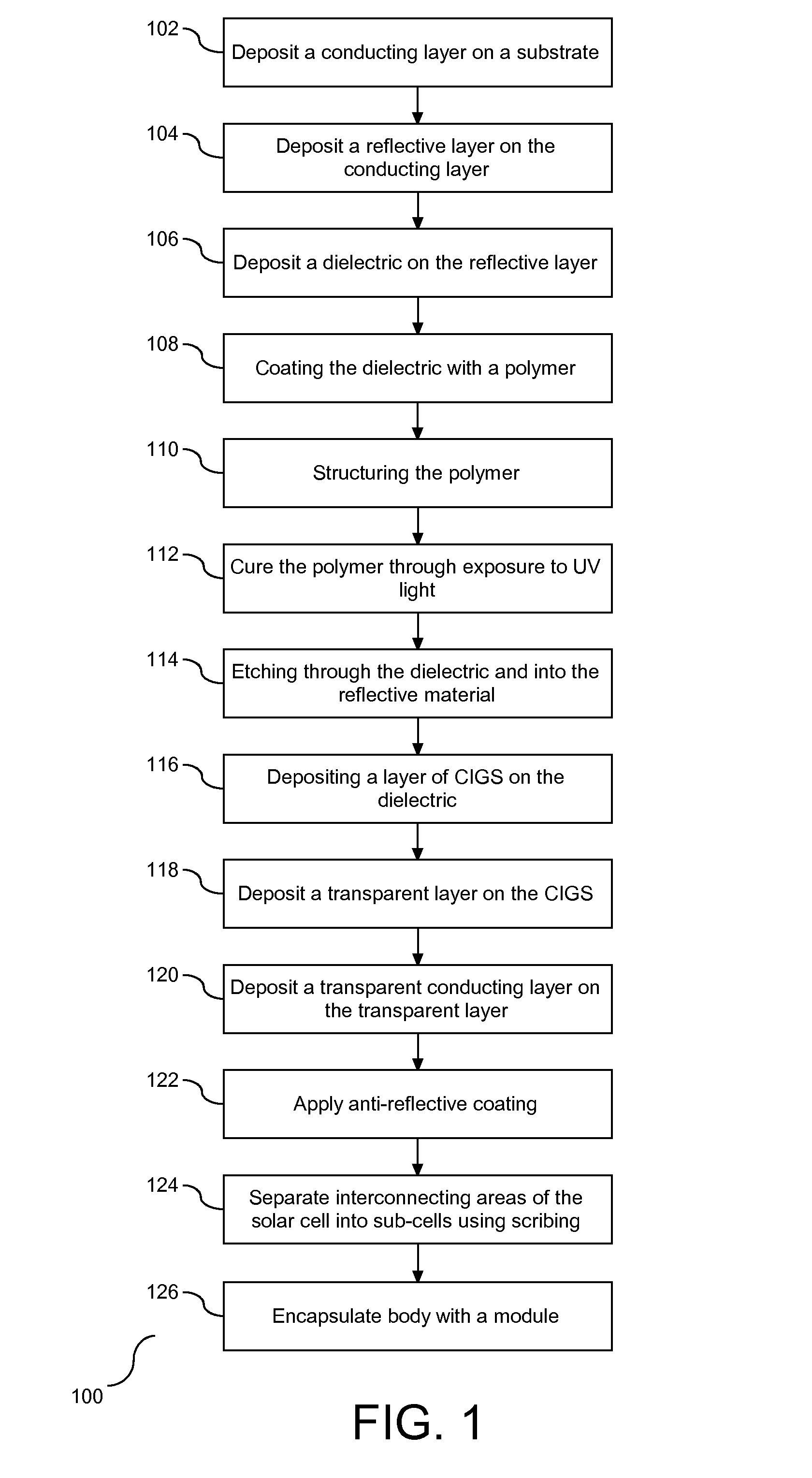
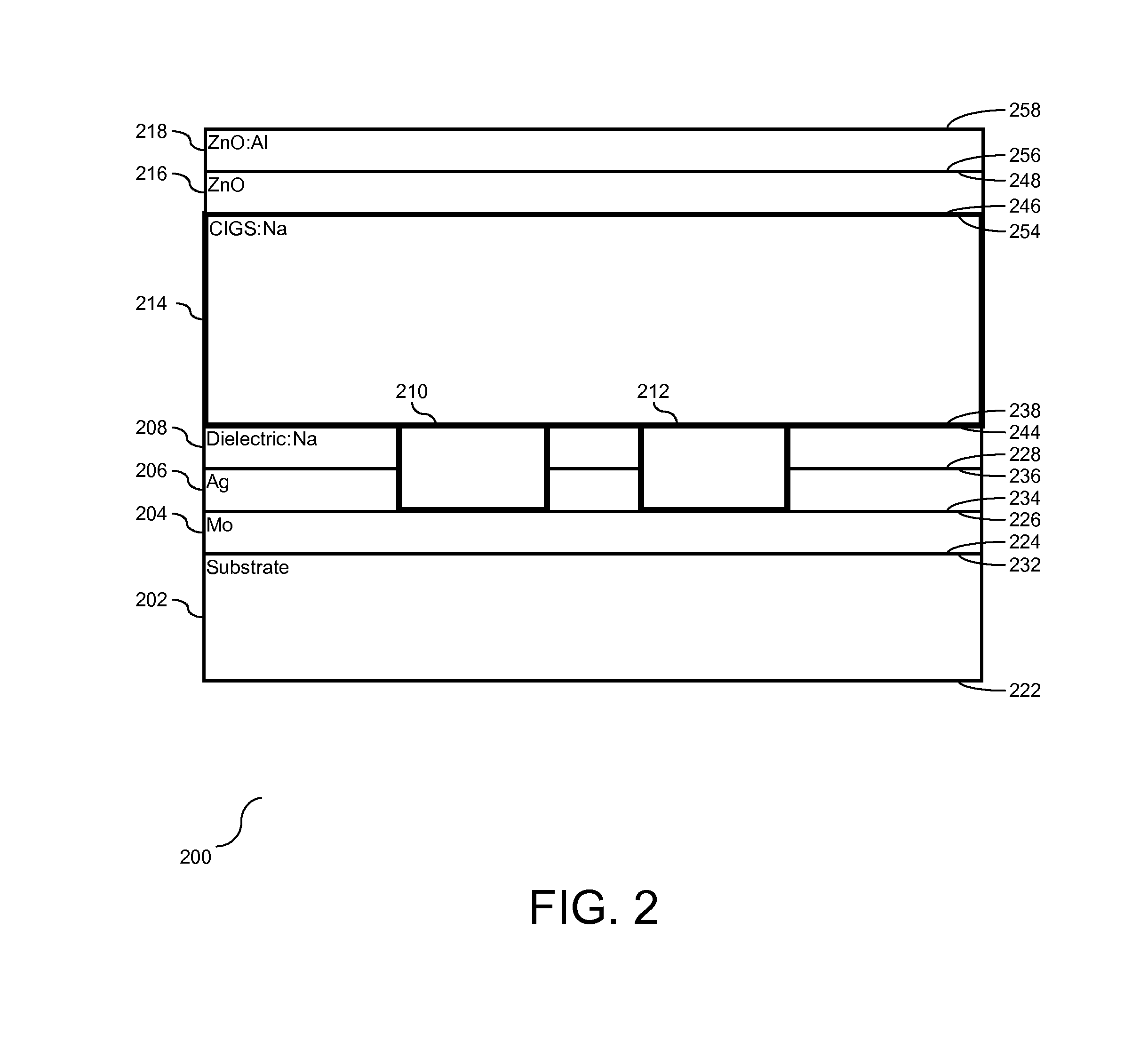
Manufacture for an improved stacked-layered thin film solar cell. Solar cell has reduced absorber thickness and an improved back contact for Copper Indium Gallium Selenide solar cells. The back contact provides improved reflectance particularly for infrared wavelengths while still maintaining ohmic contact to the semiconductor absorber. This reflectance is achieved by producing a back contact having a highly reflecting metal separated from an absorbing layer with a dielectric layer.

Description

BACKGROUND[0001]1. Technical Field[0002]The present invention relates to thin film solar cells. More specifically, the invention relates to a stacked-layered thin film solar cell with improved performance characteristics.[0003]2. Description of the Prior Art[0004]The art of solar cells addresses the conversion of radiation into electrical energy. Much research has been conducted to maximize the efficiency of a solar cell. There is a demand to further reduce the absorber thickness of a solar cell to reduce material costs, decrease the time required for deposition processing, and increase the throughput of deposition equipment. Shortcomings however, include the back contact of a solar cell having reduced reflectance for infrared wavelengths and a surface with a high probability for charge carrier recombination leading to decreased efficiency of the solar cell.SUMMARY[0005]This invention comprises a thin-film solar cell and a method for its manufacture.[0006]In one aspect, a thin-film ...

Claims


Application Information

Patent Timeline
Patent Type & Authority Applications(United States)
IPC IPC(8): H01L31/0232H01L31/0203H01L31/18H01L31/0224
CPCH01L31/022425H01L31/03923Y02E10/52Y02E10/541H01L31/0749H01L31/056Y02P70/50H01L31/02168H01L31/022433H01L31/022483H01L31/048H01L31/186H01L31/1884
Inventor EICKELMANN, HANS-JUERGENHAAG, MICHAELKELLMANN, RUEDIGERSCHMIDT, MARKUSWINDELN, JOHANNES
Owner IBM CORP
Learn More