Copper indium gallium selenide solar cell preparation method

A technology of solar cells and sodium salts, which can be used in circuits, electrical components, and final product manufacturing, etc., and can solve problems such as cracking of Na-Mo targets.

Active Publication Date: 2013-12-25
GUANMAT OPTOELECTRONICS MATERIALS INC
View PDF9 Cites 3 Cited by
  • Summary
  • Abstract
  • Description
  • Claims
  • Application Information

AI Technical Summary

Problems solved by technology

However, this method also has limitations, and the Na-Mo t

Method used


Image

  • Copper indium gallium selenide solar cell preparation method
  • Copper indium gallium selenide solar cell preparation method
  • Copper indium gallium selenide solar cell preparation method

Examples


Embodiment Construction

[0027] The detailed implementation examples mentioned in the present invention all belong to the content of the invention of the present invention. However, the present invention can be implemented in many other ways that are different from the detailed implementation examples, and those skilled in the art can make similar extensions without departing from the content of the present invention. Therefore, any simple modifications, equivalent changes and modifications made to the above embodiments according to the technical essence of the present invention still belong to the protection scope of the technical solution of the present invention.

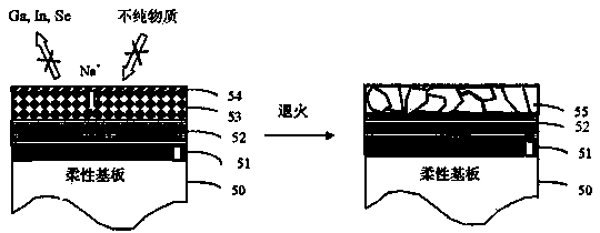
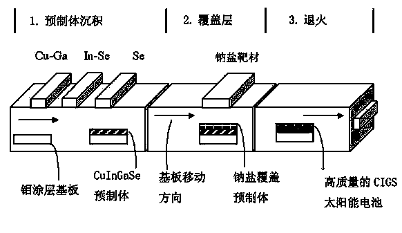
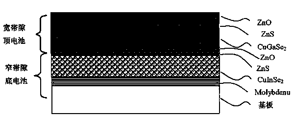
[0028] The invention provides a method for manufacturing IB-IIIA-VIA semiconductor compound, the semiconductor compound obtained by the method has good crystal grains and can be applied to the manufacture of CIGS thin film batteries. The general purpose of the present invention is to provide a kind of preparation method of copper indium ...


PUM

PropertyMeasurementUnit
Thicknessaaaaaaaaaa
Sheet resistanceaaaaaaaaaa

Abstract

The invention provides a copper indium gallium selenide solar cell preparation method. The copper indium gallium selenide solar cell preparation method comprises the following steps: a substrate of a first electrode film is obtained and deposited; a mixed precursor layer is formed on the substrate, wherein a mixed precursor is composed of elements in a I B group, a III A group and a IV A group according to an ideal quantity relative ratio of a product; a cover top layer containing sodium salt is deposited on the mixed precursor layer; the mixed precursor layer and the cover top layer containing the sodium salt are heated and annealed together to form a high-quality I B-III A-VI A semiconductor absorption layer. Due to the addition of the cover top layer containing the sodium salt, on one hand, loss of metallic elements and selenium can be prevented, and contamination by harmful impure substance is prevented; on the other hand, a polycrystal thin-film I B-III A-IV A semiconductor absorption layer structure can be further improved, and the copper indium gallium selenide solar cell preparation method can be applied to the I B-III A-VI A semiconductor absorption layer in large-area photovoltaic production.

Description

technical field [0001] The invention relates to the field of semiconductor devices, in particular to a method for preparing IB-IIIA-VI semiconductor compound solar cells, which can be used in the manufacturing process of thin-film photovoltaic devices or solar cell absorbing layers. Background technique [0002] Copper indium diselenide and its derivatives substituted by gallium and sulfur are direct gap semiconductor materials, abbreviated as CuIn x Ga 1-x Se 2 S 2-Y (where 0≤x≤1, O≤y≤2) or CIS, CIGSe or CIGSeS. These compounds belong to IB-IIIA-VIA group materials, and are widely used in the field of thin-film solar cells because of their good photoelectric performance, stable performance and high energy conversion efficiency. In addition, because of its light absorption coefficient higher than that of other photovoltaic cell materials, the thickness of the CIGS cell absorber layer can be less than 2.5 μm. Copper indium diselenide and its gallium and sulfur substitute...

Claims


Application Information

Patent Timeline
IPC IPC(8): H01L31/18H01L31/0224
CPCY02P70/50
Inventor 李晓常
Owner GUANMAT OPTOELECTRONICS MATERIALS INC
Why Eureka
Try Eureka