Photovoltaic cell structure

a photovoltaic cell and cell structure technology, applied in the direction of sustainable manufacturing/processing, climate sustainability, semiconductor devices, etc., can solve the problems of contaminated environment, human health impacted, and toxic cadmium if eaten, so as to achieve less harmful to the environment

Inactive Publication Date: 2011-12-08
PVNEXT CORP
View PDF4 Cites 2 Cited by
  • Summary
  • Abstract
  • Description
  • Claims
  • Application Information

AI Technical Summary

Benefits of technology

[0012]In an embodiment, the n-type semiconductor layer may include titanium oxide (TiO2) or tungsten oxide (WO3) and have a thickness between 1 and 1000 nm. For example, titanium oxide becomes active

Problems solved by technology

Cadmium is toxic and is severely harmful to human beings if eaten.
If photovoltaic cells include cadmium, e.g., the buffer layers include CdS, and used photovoltaic cells are not properly disposed, the environment will be contami

Method used


Image

  • Photovoltaic cell structure
  • Photovoltaic cell structure
  • Photovoltaic cell structure

Examples


first embodiment

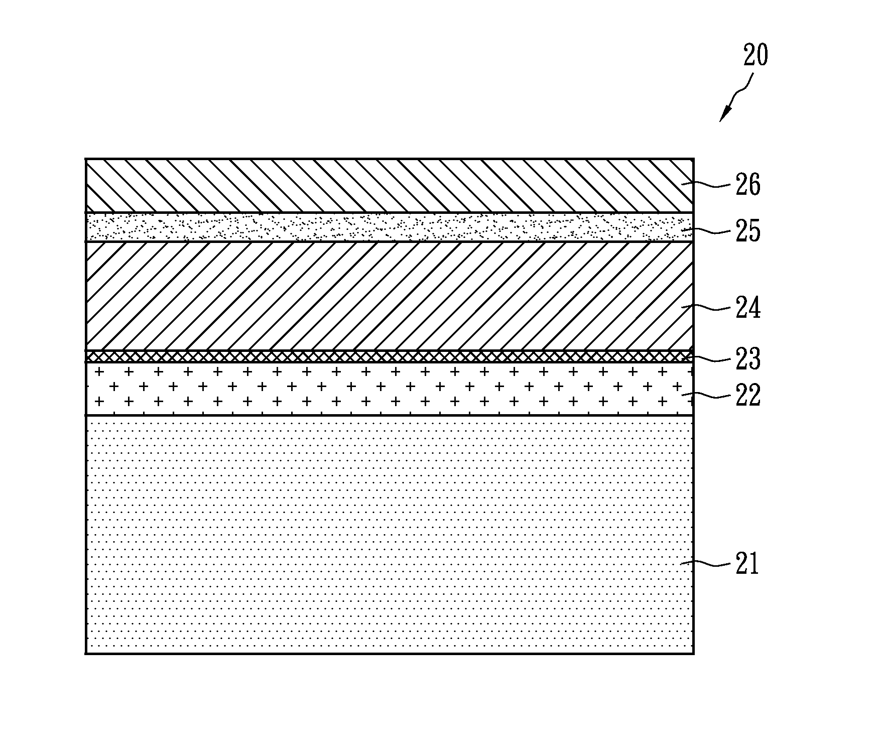
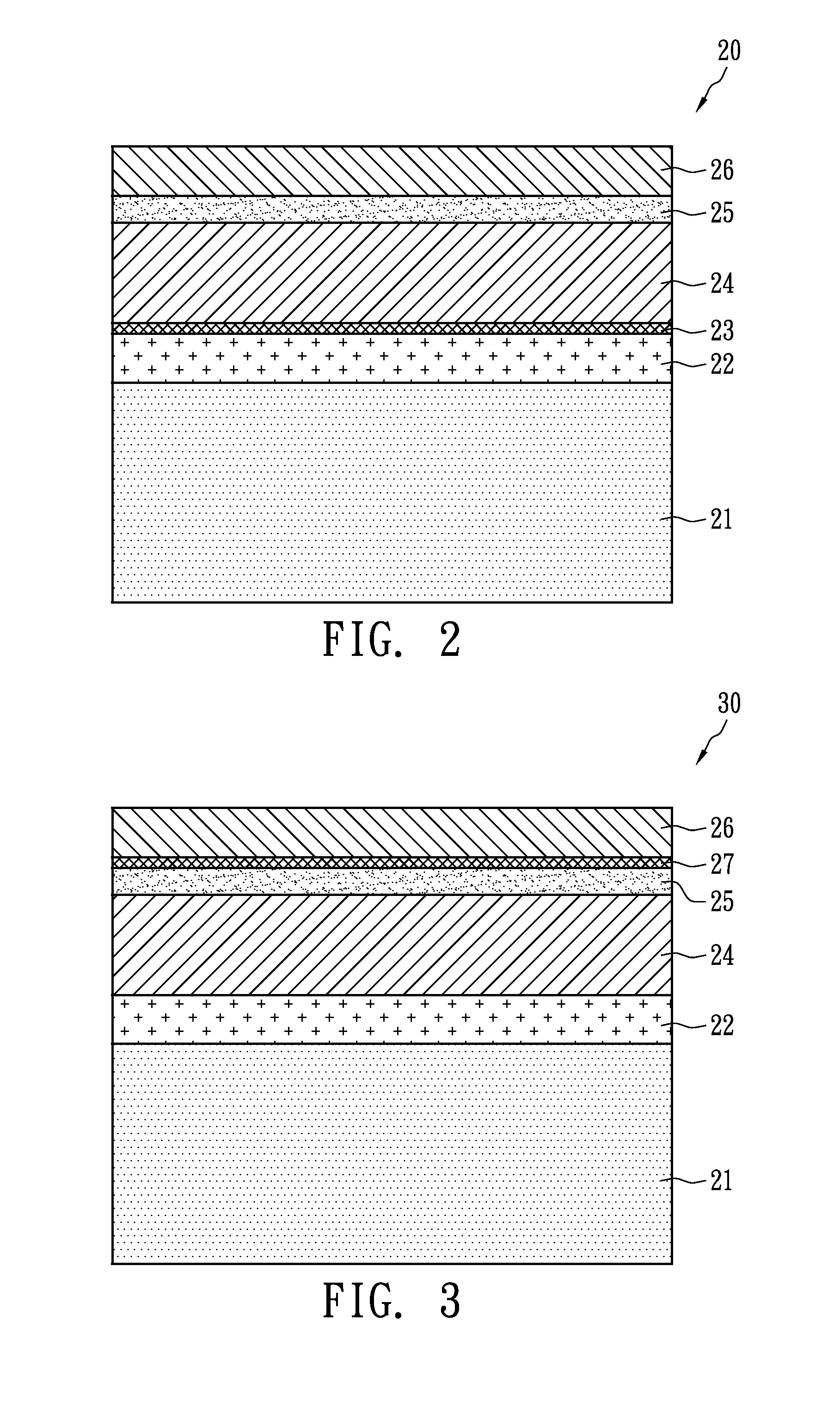
[0017]FIG. 2 shows a photovoltaic cell structure in accordance with the present invention. A photovoltaic cell structure 20 is a laminated structure and includes a substrate 21, a metal layer 22, a high resistivity layer 23, a p-type semiconductor layer 24, an n-type semiconductor layer 25 and a transparent conductive layer 26. In addition to a glass substrate, the substrate 21 may be a polyimide flexible substrate, or a metal plate or a metal foil of stainless steel, molybdenum, copper, titanium or aluminum. The substrate 21 is used for film formation and the shape thereof is not restricted to a plate; others such as a ball or specific or arbitrary shapes can also be used. The metal layer 22 may be a molybdenum, chromium, vanadium or tungsten layer of a thickness between 0.5 and 1 μm formed on the surface of the substrate 21 to create a back contact metal layer of the cell. The high resistivity layer 23 is formed on the metal layer 22 and has a thickness preferably between 25 and 2...

second embodiment

[0020]FIG. 3 shows a photovoltaic cell structure in accordance with the present invention. A photovoltaic cell structure 30 is a laminated structure and includes a substrate 21, a metal layer 22, a p-type semiconductor layer 24, an n-type semiconductor layer 25, a high resistivity layer 27 and a transparent conductive layer 26. In comparison with the photovoltaic cell structure 20 shown in FIG. 2, the position of the high resistivity layer 27 is changed. The high resistivity layer 23 is initially placed between the metal layer 22 and the p-type semiconductor layer 24. Instead, the high resistivity layer 27 is placed between the n-type semiconductor layer 25 and the transparent conductive layer 26. In an embodiment, the high resistivity layer 27 comprises zinc oxide, which is also insulative for prevention of electrical shorts of devices. Likewise, the n-type semiconductor layer 25 can be made of photo catalyst material such as titanium oxide or tungsten oxide. In one embodiment of t...


PUM


Abstract

A photovoltaic cell structure includes a substrate, a metal layer, a p-type semiconductor layer, an n-type semiconductor layer, a transparent conductive layer and a high resistivity layer. The metal layer is formed on the substrate. The p-type semiconductor layer is formed on the metal layer and may include a compound of copper indium gallium selenium sulfur (CIGSS), copper indium gallium selenium (CIGS), copper indium sulfur (CIS), copper indium selenium (CIS) or a compound of at least two of copper, selenium or sulfur. The n-type semiconductor layer exhibits photo catalyst behavior that can increase carrier mobility by receiving light, and is formed on the p-type semiconductor layer, thereby forming a p-n junction. The transparent conductive layer is formed on the n-type semiconductor layer. The high resistivity layer is formed between the metal layer and the transparent conductive layer.

Description

CROSS REFERENCE TO RELATED APPLICATIONS[0001]This application is a Continuation-in-part application of U.S. application Ser. No. 12 / 507,930 filed Jul. 23, 2009.BACKGROUND OF THE INVENTION[0002](A) Field of the Invention[0003]The present invention relates to a photovoltaic cell structure, and more specifically, to a thin-film photovoltaic cell structure including Copper Indium Gallium Selenium (CIGS) or Copper Indium Selenium (CIS).[0004](B) Description of the Related Art[0005]Normally, Copper Indium Gallium Diselenide thin-film solar cells are one of two types; one is comprised of copper, indium and selenium, and another is comprised of copper, indium, gallium and selenium. Because of the high photoelectrical efficiency and low material cost, solar cell development is expected to continue at a rapid pace. The photoelectrical efficiency of CIGS solar cells in the laboratory can reach around 19%, and 13% for related solar cell modules.[0006]FIG. 1 shows a traditional CIGS photovoltaic...

Claims


Application Information

Patent Timeline
IPC IPC(8): H01L31/0224H01L31/02
CPCH01L31/022425H01L31/032Y02E10/541H01L31/03928H01L31/0749H01L31/0392H01L31/03925Y02P70/50
Inventor CHANG, FENG FANLIN, HSIN HUNGLIN, HSIN CHIHHSIEH, CHI HUALEE, TSUNG LUNG
Owner PVNEXT CORP
Why Eureka
Try Eureka