Semiconductor device and method for manufacturing the same

Active Publication Date: 2014-04-17
SEMICON ENERGY LAB CO LTD
View PDF3 Cites 14 Cited by
  • Summary
  • Abstract
  • Description
  • Claims
  • Application Information

AI Technical Summary

Benefits of technology

[0024]According to one embodiment of the present invention, a miniaturized transistor including

Problems solved by technology

However, short channel length of a transistor causes a decrease i

Method used


Image

  • Semiconductor device and method for manufacturing the same
  • Semiconductor device and method for manufacturing the same
  • Semiconductor device and method for manufacturing the same

Examples


application example

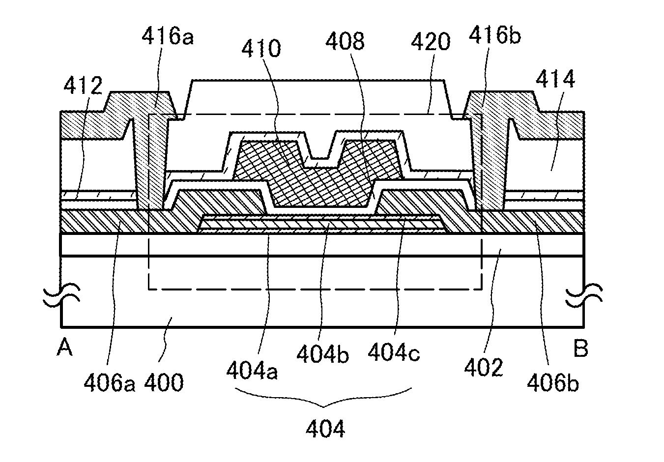
[0212]As an example of a semiconductor device, a circuit diagram of a NOR circuit, which is a logic circuit, in which any of the above transistors can be used is illustrated in FIG. 6A. FIG. 6B is a circuit diagram of a NAND circuit.

[0213]In the NOR circuit illustrated in FIG. 6A, p-channel transistors 801 and 802 each have a structure in which a single crystal silicon substrate is used for the channel formation region, and n-channel transistors 803 and 804 each have a structure which is similar to the structure of any of the transistors 420, 430, 440, and 450 and in which an oxide semiconductor layer is used for the channel formation region.

[0214]In the NOR circuit illustrated in FIG. 6A, a conductive layer controlling the electrical characteristics of the transistor may be provided to overlap with a gate electrode layer with an oxide semiconductor layer provided therebetween in each of the transistors 803 and 804. By controlling the potential of the conductive layer to a potential...

example 1

[0282]In this example, silicon oxynitride films which can be used as a gate insulating layer included in a semiconductor device of one embodiment of the present invention were fabricated, and characteristics thereof were evaluated.

[0283]First, a method for fabricating samples is described.

[0284]A 100-nm-thick silicon oxynitride film was formed over a quartz substrate. The silicon oxynitride film was formed under the following conditions: the substrate was placed in a treatment chamber of a plasma CVD apparatus, silane with a flow rate of 1 sccm and dinitrogen monoxide with a flow rate of 800 sccm as a source gas were supplied to the treatment chamber, and a power of 150 W was supplied with the use of a 60 MHz high-frequency power source. Further, the temperature of the substrate at the formation of the silicon oxynitride film was 350° C. Note that the plasma CVD apparatus used in this example is a parallel-plate plasma CVD apparatus in which the electrode area is 615 cm2 and the den...

example 2

[0296]In this example, silicon oxynitride films which can be used as a gate insulating layer included in a semiconductor device of one embodiment of the present invention were fabricated, and characteristics thereof were evaluated.

[0297]A 100-nm-thick silicon oxynitride film was formed over a silicon substrate. Conditions for forming the silicon oxynitride film were similar to those in Example 1. Here, the silicon oxynitride film was deposited at a pressure of 200 Pa for Sample F1, 100 Pa for Sample F2, and 40 Pa for Comparative Sample F3.

[0298]FIGS. 21A to 21C show the TDS results of Sample F1, Sample F2, and Comparative Sample F3. In the TDS analysis, the ion intensity of a gas detected at m / z=2 (e.g., H2) was measured. FIG. 21A, FIG. 21B, and FIG. 21C show the results of Sample F1, Sample F2, and Comparative Sample F3, respectively.

[0299]Similarly, FIGS. 22A to 22C show the TDS results of Sample F1, Sample F2, and Comparative Sample F3. In the TDS analysis, the ion intensity of a...


PUM


Abstract

Stable electrical characteristics and high reliability are provided for a miniaturized semiconductor device including an oxide semiconductor, and the semiconductor device is manufactured. The semiconductor device includes a base insulating layer; an oxide stack which is over the base insulating layer and includes an oxide semiconductor layer; a source electrode layer and a drain electrode layer over the oxide stack; a gate insulating layer over the oxide stack, the source electrode layer, and the drain electrode layer; a gate electrode layer over the gate insulating layer; and an interlayer insulating layer over the gate electrode layer. In the semiconductor device, the defect density in the oxide semiconductor layer is reduced.

Description

BACKGROUND OF THE INVENTION[0001]1. Field of the Invention[0002]The present invention relates to an object, a method, a manufacturing method, a process, a machine, manufacture, or a composition of matter. In particular, one embodiment of the present invention relates to a semiconductor device, a display device, a light-emitting device, a driving method thereof, or a manufacturing method thereof.[0003]In this specification, a semiconductor device generally means a device which can function by utilizing semiconductor characteristics. Electro-optical devices, display devices, memory devices, semiconductor circuits, and electronic devices are in some cases included in semiconductor devices and in other cases include semiconductor devices.[0004]2. Description of the Related Art[0005]Attention has been focused on a technique for forming a transistor using a semiconductor layer (also referred to as a thin film transistor (TFT)). The transistor is applied to a wide range of electronic devic...

Claims


Application Information

Patent Timeline
IPC IPC(8): H01L29/66
CPCH01L29/66765H01L29/66969H01L29/7869H01L21/02274H01L29/4908H01L29/66742H01L21/28185H01L21/28194H01L21/823462H01L21/823857H01L29/1054H01L29/42384H01L29/78
Inventor TEZUKA, SACHIAKITANAKA, TETSUHIROTAKEUCHI, TOSHIHIKOSUZAWA, HIDEOMIHONDO, SUGURU
Owner SEMICON ENERGY LAB CO LTD
Why Eureka
Try Eureka