Conductive structure of transparent conductive film, transparent conductive film and preparation method thereof

a technology of transparent conductive film and conductive structure, which is applied in the direction of dielectric characteristics, conductive layers on insulating supports, instruments, etc., can solve the problems of insufficient change, complex and long process, and in the manufacturing process to achieve the effect of reducing the thickness of the entire multi-touch display devi

Inactive Publication Date: 2014-05-01
NANCHANG O FILM TECH CO LTD
View PDF7 Cites 17 Cited by
  • Summary
  • Abstract
  • Description
  • Claims
  • Application Information

AI Technical Summary

Benefits of technology

[0008]In view of this, a first purpose of the present invention is to provide a single-sided double-layer graphic conductive structure, making the transparent conductive film having the conductive structure support the multi-touch function. A second purpose of the present invention is to provide a transparent conductive film having the above conductive structure and the preparation method thereof, which can not only support the multi-touch function but also consumedly reduce the thickness of the entire multi-touch display device.

Problems solved by technology

Although the touchscreen manufacturing technology develops rapidly, the ITO layer based manufacturing process, taking the projected capacitive screen for example, has not changed much in recent years.
The traditional production process is complex and lengthy, and therefore yield control has become an unavoidable problem in the field of touchscreen manufacturing at the present stage.
In addition, an etching process also inevitably needs to be used in the approach, which will waste a great deal of ITO and metal materials.
Therefore, how to achieve a simple and environmental protective process of manufacturing the transparent conductive film is a key technical problem that urgently needs to be solved.
However, the single-layer transparent conductive film is difficult to support the multi-touch technology.
However, the solution of using two pieces of the transparent conductive film has the following defects: Firstly, jump wire is realized mainly by using yellow light, which has a complicated process; besides, the jump wire is visible on the touchscreen, which will affect the appearance.
Secondly, the development direction of the existing touchscreen is to be lighter and thinner; if one layer of the conductive film is added, i.e. a double-layer conductive film is used for touching, thickness and weight will certainly be bound to increase at the expense, which does not meet the development trend.

Method used


Image

  • Conductive structure of transparent conductive film, transparent conductive film and preparation method thereof
  • Conductive structure of transparent conductive film, transparent conductive film and preparation method thereof
  • Conductive structure of transparent conductive film, transparent conductive film and preparation method thereof

Examples


example 1

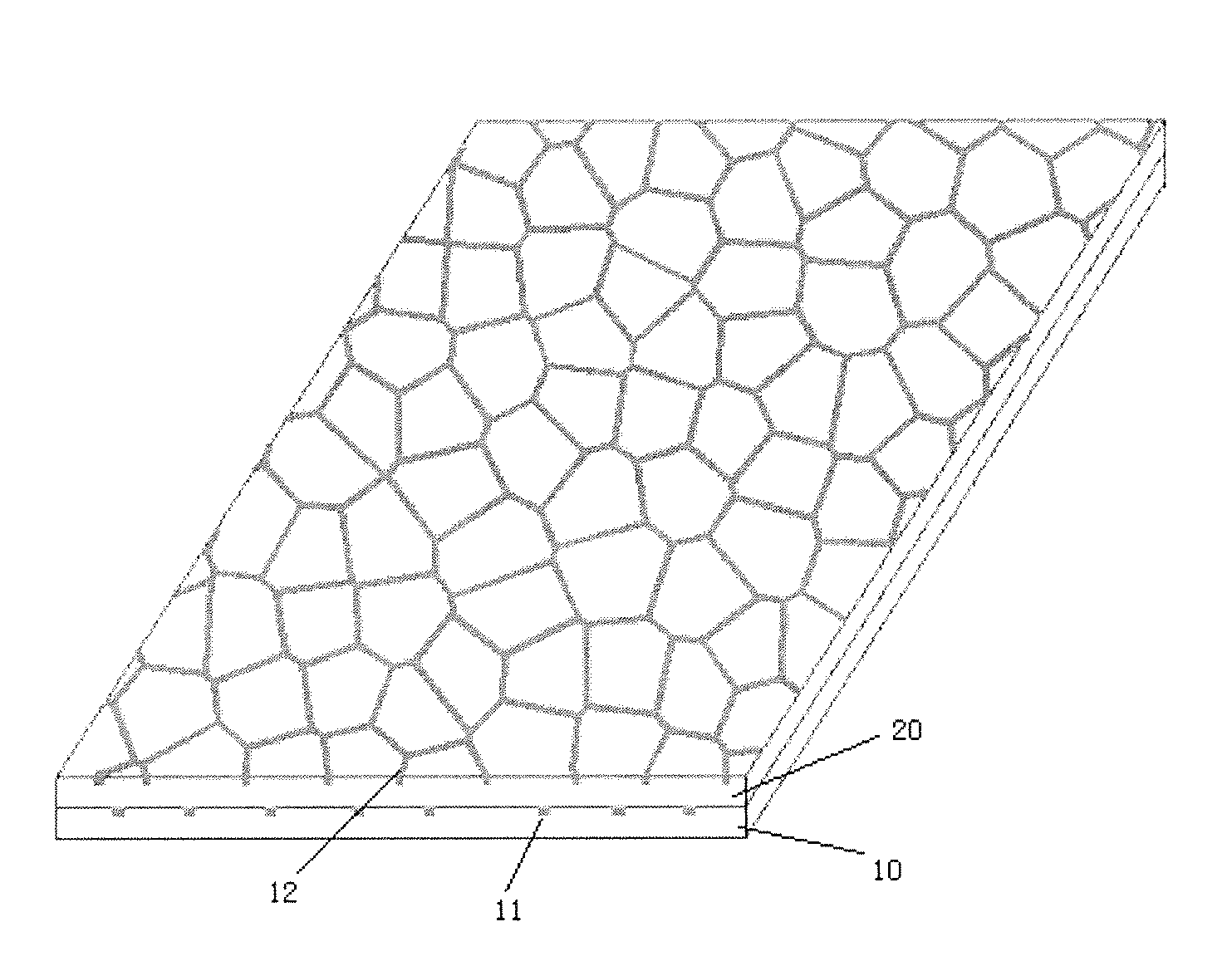
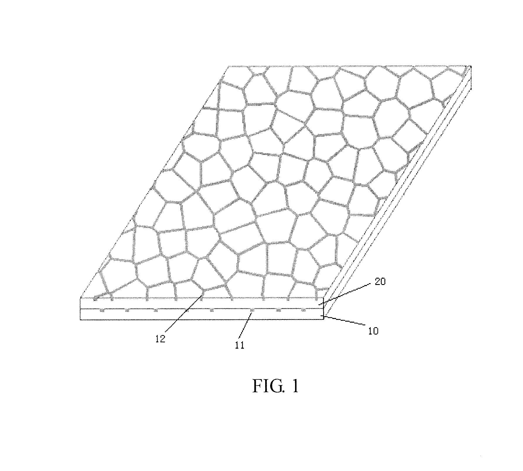
[0042]Referring to FIG. 1, which is a schematic diagram of part of the transparent conductive film of the first embodiment of the present invention. In this embodiment, the first metal embedded layer in the conductive structure is directly prepared on the substrate, as shown in the diagram, the transparent conductive film includes a transparent substrate 10 and a transparent polymer layer 20 arranged on the substrate. The conductive structure includes a grid-shaped first metal embedded layer 11 arranged in the substrate 1, and a grid-shaped second metal embedded layer 21 arranged in the transparent polymer layer 20; in order to ensure the first metal embedded layer 11 and the second metal embedded layer 21 to be insulated from each other, the thickness of the second metal embedded layer 21 is made to be less than that of the polymer layer 20, thereby part of the polymer layer 20 being arranged between the first metal embedded layer 11 and the second metal embedded layer 21 and thus ...

example 2

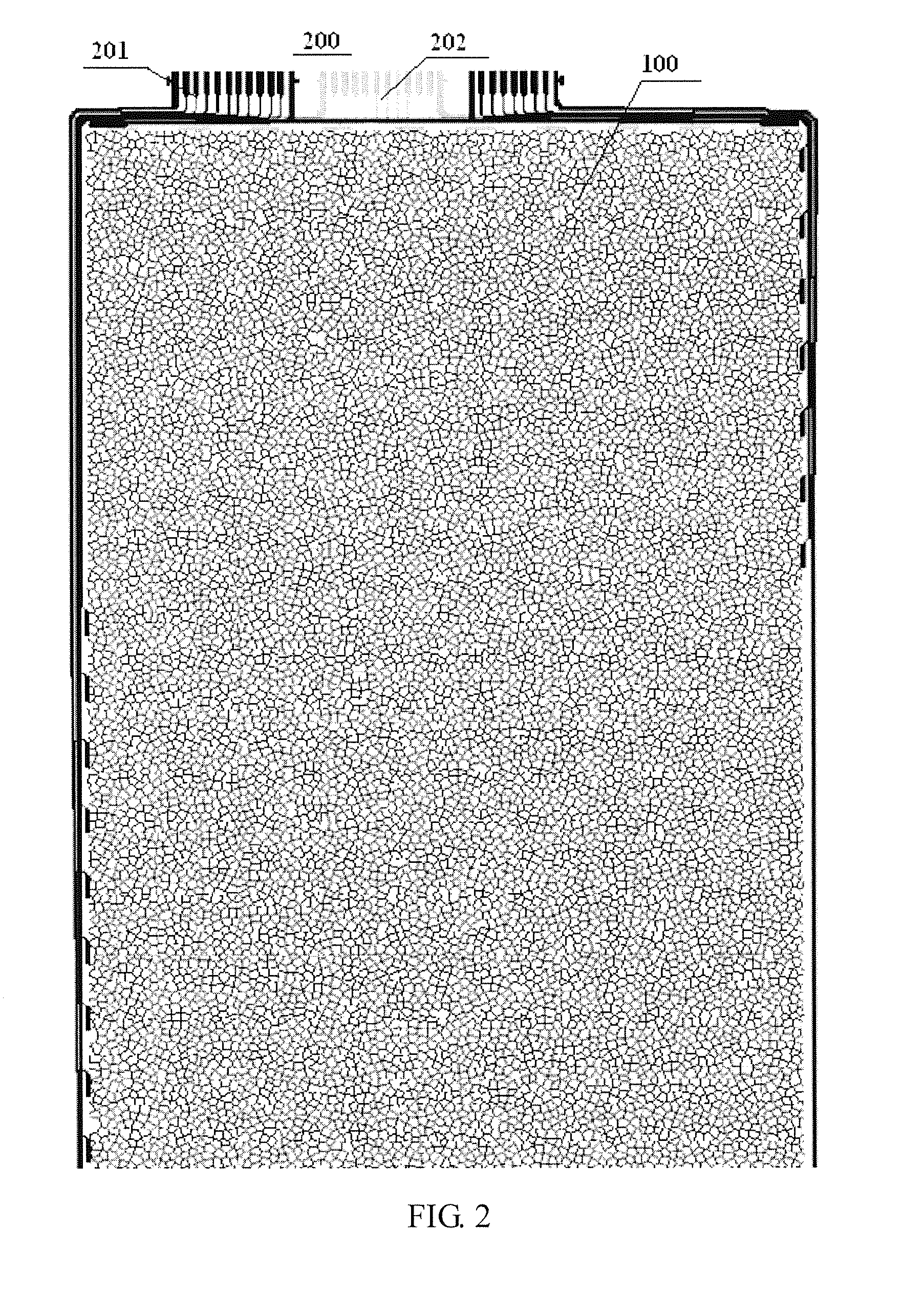
[0052]Referring to FIG. 8, which is a schematic diagram of part of the transparent conductive film of the second embodiment of the present invention. In the embodiment, the first metal embedded layer in the conductive structure is directly prepared in the first polymer layer on the substrate. As shown in the diagram, the transparent conductive film includes a transparent substrate 10′, a transparent first polymer layer 20′ located on the substrate, and a transparent second polymer layer 30 located on the first polymer layer 20′. The conductive structure includes a grid-shaped first metal embedded layer 11′ arranged in the first polymer layer 20′, and a grid-shaped second metal embedded layer 21′ arranged in the second transparent polymer layer 30. In order to ensure the first metal embedded layer 11′ and the second metal embedded layer 21′ to be insulated from each other, the thickness of the second metal embedded layer 21′ is made to be less than that of the second polymer layer 30...


PUM

PropertyMeasurementUnit
transmittanceaaaaaaaaaa
stepper angleaaaaaaaaaa

Abstract

The present invention discloses a conductive structure of a transparent conductive film, the transparent conductive film and a preparation method thereof, wherein the transparent conductive film has a single-sided double-layer conductive structure, which includes a first metal embedded layer embossed on the substrate or on the polymer layer on the surface of the substrate, and a second metal embedded layer embossed on the polymer material applied onto the surface of the first metal embedded layer. The first and second layers of the conductive structure have a grid recess structure, with all the recesses filled with the conductive material. The single-sided double-layer graphic transparent conductive film provided by the present invention has a high resolution, a high transmittance, an independently adjustable sheet resistance, and many other advantages. The transparent conductive film can reduce the cost as well as weight and thickness of the touch panel.

Description

FIELD OF THE INVENTION[0001]The present invention relates to the field of multi-touch display, and particularly relates to a transparent conductive film supporting the multi-touch technology and the preparation method thereof.BACKGROUND OF THE INVENTION[0002]The transparent conductive film is a film having good electrical conductivity, and a high visible light transmittance. The transparent conductive film has been widely used in flat panel displays, photovoltaic devices, touch panels and electromagnetic shielding, and other fields, having a very broad market space.[0003]An ITO layer is a vital component in the touchscreen module. Although the touchscreen manufacturing technology develops rapidly, the ITO layer based manufacturing process, taking the projected capacitive screen for example, has not changed much in recent years. ITO coating, graphic ITO, and transparent electrode silver wire production are always inevitably needed. The traditional production process is complex and le...

Claims


Application Information

Patent Timeline
Patent Type & Authority Applications(United States)
IPC IPC(8): H05K1/02
CPCH05K1/0213G06F3/0445H05K3/1258H05K2201/0108H05K2201/09681G06F3/041G06F2203/04103H01B5/14
Inventor GAO, YULONGCUI, ZHENGSUN, CHAO
Owner NANCHANG O FILM TECH CO LTD
Why Eureka
Try Eureka