Multigate field effect transistor and process thereof

a field effect transistor and multi-gate technology, applied in the direction of basic electric elements, electrical equipment, semiconductor devices, etc., can solve the problems of degrading the electrical performance of the multi-gate field effect transistor, and achieve the effect of reducing processing costs and parasitic capacitan

Active Publication Date: 2014-05-01
UNITED MICROELECTRONICS CORP
View PDF6 Cites 49 Cited by
  • Summary
  • Abstract
  • Description
  • Claims
  • Application Information

AI Technical Summary

Benefits of technology

[0006]The present invention provides a multigate field effect transistor and a process thereof, which forms voids in a dielectric layer between two fin-shaped structures, so that the parasitic capacitances of the multigate field effect transistor can be reduced, and the aforesaid problem can therefore be solved.
[0009]According to the above, the present invention provides a multigate field effect transistor and a process thereof, which forms voids in a dielectric layer between two fin-shaped structures, so that the parasitic capacitances of the multigate field effect transistor, especially between the fin-shaped structures, can be reduced. Moreover, processes for forming a dielectric layer with voids in the dielectric layer between the fin-shaped structures in the present invention can reduce processing costs compared to processes intended to fully fill the dielectric layer (with no voids).

Problems solved by technology

However, assizes of multigate field effect transistors shrink, the parasitic capacitances between each of the fin-shaped structures become large and degrade electrical performances of the multigate field effect transistors.

Method used


Image

  • Multigate field effect transistor and process thereof
  • Multigate field effect transistor and process thereof
  • Multigate field effect transistor and process thereof

Examples


first embodiment

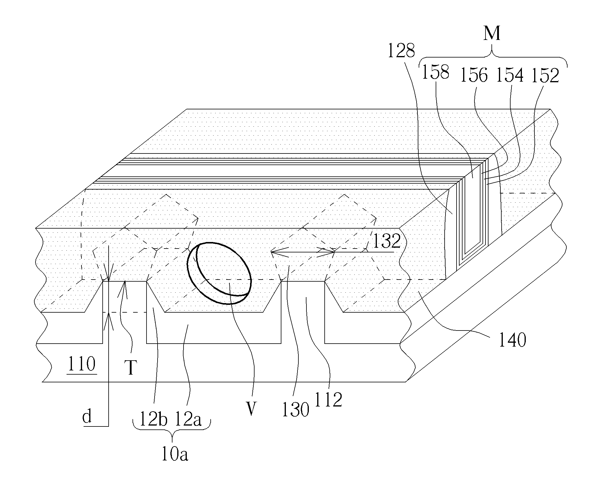
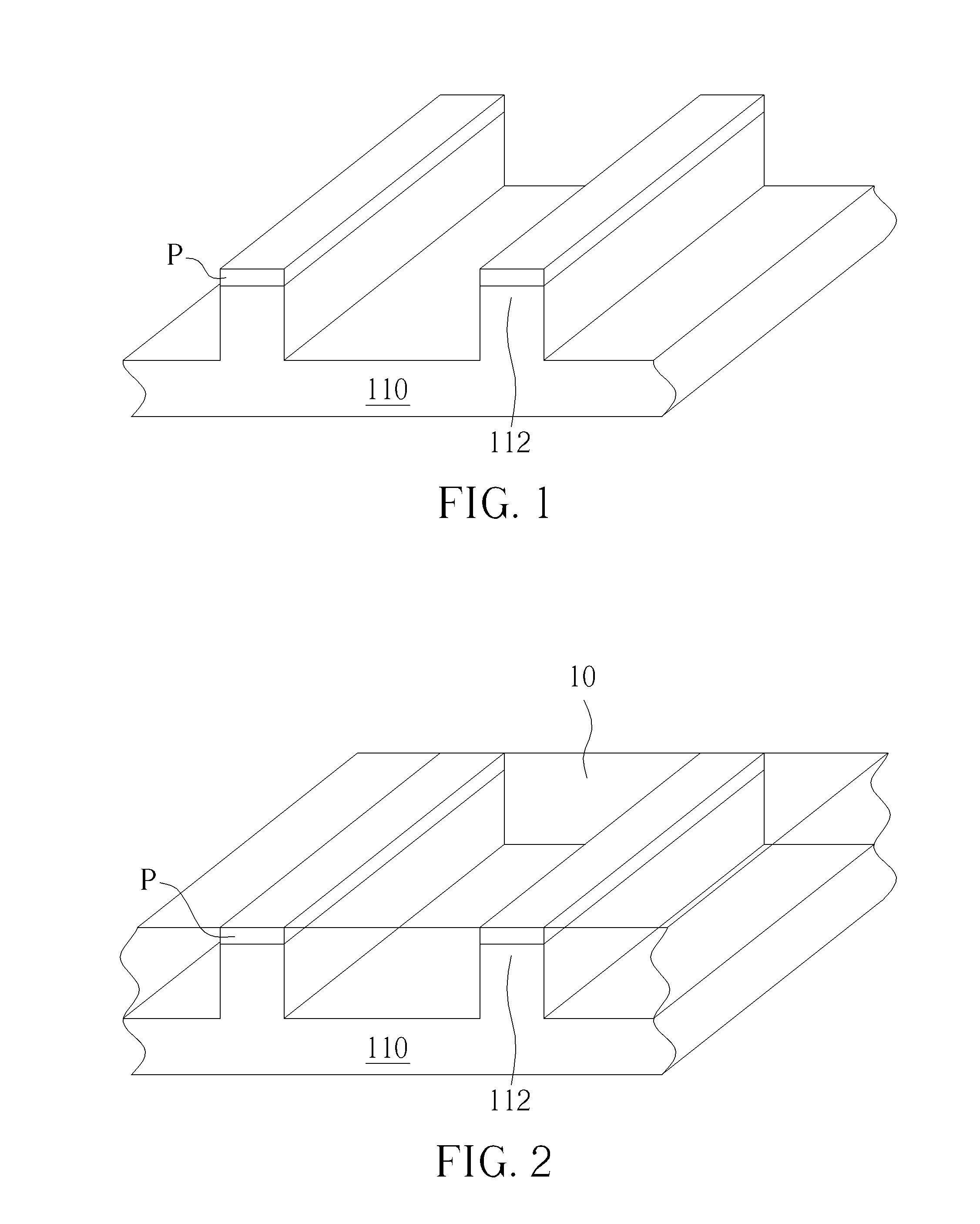
[0015]FIGS. 1-7 schematically depict cross-sectional views of a multigate field effect transistor process according to the present invention. A plurality of fin-shaped structures is formed on a substrate. As shown in FIG. 1, two fin-shaped structures 112 are formed on a substrate 110. The substrate 110 may be a semiconductor substrate such as a silicon substrate, a silicon containing substrate, a III-V group-on-silicon (such as GaN-on-silicon) substrate, a graphene-on-silicon substrate or a silicon-on-insulator (SOI) substrate. In details, the method of forming the two fin-shaped structures 112 on the substrate 110 may include the following steps. A bulk bottom substrate (not shown) is provided. A hard mask layer (not shown) is formed on the bulk bottom substrate (not shown) and is patterned to define the location of the fin-shaped structures 112, which will be formed in the bulk bottom substrate (not shown). An etching process is performed to form the fin-shaped structures 112 in t...

second embodiment

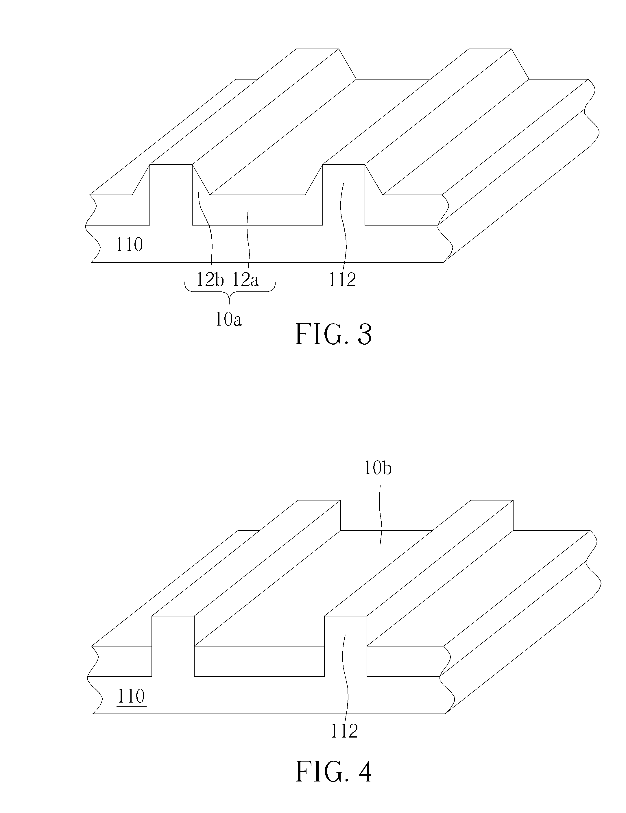
[0028]FIGS. 8-9 schematically depict cross-sectional views of a multigate field effect transistor process according to the present invention. The previous processes of this embodiment are common to the former embodiment (as shown in FIGS. 1-2), including two fin-shaped structures 112 formed on a substrate 110 (as shown in FIG. 1); an isolation structure 10 is formed on the substrate 110 between the two fin-shaped structures 112 (as shown in FIG. 2). Then, an epitaxial structure 130 is formed on each of the fin-shaped structures 112 without etching back the isolation structure 10 first as shown in FIG. 8. Thereafter, the isolation structure 10 is etched back to form an isolation structure 10a as shown in FIG. 9. It is worth noting that, the isolation structure 10a including a bottom part 12a and the two sidewall parts 12b are formed in the former embodiment to isolate the fin-shaped structures 112, enabling the epitaxial structures 130 to grow upward so that the voids V can be formed...


PUM


Abstract

A multigate field effect transistor includes two fin-shaped structures and a dielectric layer. The fin-shaped structures are located on a substrate. The dielectric layer covers the substrate and the fin-shaped structures. At least two voids are located in the dielectric layer between the two fin-shaped structures. Moreover, the present invention also provides a multigate field effect transistor process for forming said multigate field effect transistor including the following steps. Two fin-shaped structures are formed on a substrate. A dielectric layer covers the substrate and the two fin-shaped structures, wherein at least two voids are formed in the dielectric layer between the two fin-shaped structures.

Description

BACKGROUND OF THE INVENTION[0001]1. Field of the Invention[0002]The present invention relates generally to a multigate field effect transistor and a process thereof, and more specifically to a multigate field effect transistor and a process thereof that forms voids in a dielectric layer between fin-shaped structures.[0003]2. Description of the Prior Art[0004]With increasing miniaturization of semiconductor devices, various multi-gate MOSFET devices have been developed. The multi-gate MOSFET is advantageous for the following reasons. First, manufacturing processes of multi-gate MOSFET devices can be integrated into traditional logic device processes, and thus are more compatible. In addition, since the three-dimensional structure of the multi-gate MOSFET increases the overlapped area between the gate and the substrate, the channel region is controlled more effectively. This therefore reduces drain-induced barrier lowering (DIBL) effect and short channel effect. Moreover, the channel ...

Claims


Application Information

Patent Timeline
Patent Type & Authority Applications(United States)
IPC IPC(8): H01L21/336H01L29/78
CPCH01L29/66795H01L21/764H01L29/785H01L29/66484H01L21/02225H10B10/00
Inventor LIU, CHIH-CHIENWU, CHUN-YUANLIN, CHIN-FUCHIEN, CHIN-CHENGHSU, CHIA-LIN
Owner UNITED MICROELECTRONICS CORP
Why Eureka
Try Eureka