Insulated gate bipolar transistor

a bipolar transistor and gate technology, applied in the field of power semiconductor devices, can solve the problems of high on-state loss of devices due to a plurality of effects, low cell packing density of high-voltage devices, and low cell packing density, and achieve the effect of higher doping concentration

Active Publication Date: 2014-05-08
HITACHI ENERGY SWITZERLAND AG
View PDF6 Cites 18 Cited by
  • Summary
  • Abstract
  • Description
  • Claims
  • Application Information

AI Technical Summary

Benefits of technology

[0017]An exemplary embodiment provides an insulated gated bipolar transistor (IGBT) having layers between an emitter electrode on an emitter side and a collector electrode on a collector side opposite to the emitter side. The exemplary IGBT includes a drift layer of a first conductivity type, and a collector layer of a second conductivity type different than the first conductivity type. The collector layer is arranged between the drift layer and the collector electrode and electrically contacts the collector electrode. The exemplary IGBT also includes a base layer of a second conductivity type, where the base layer is arranged between the drift layer and the emitter electrode, and the base layer electrically contacts the emitter electrode. In addition, the exemplary IGBT includes a first source region of the first conductivity type. The first source region is arranged on the base layer towards the emitter side and electrically contacts the emitter electrode. The first source region has a higher doping concentration than the drift layer. The exemplary IGBT also includes a trench gate electrode arranged lateral to the base layer and extending deeper into the drift layer than the base layer. The trench gate electrode is separated from the base layer, the first source region and the drift layer by a first insulating layer. A channel is formable between the emitter electrode, the first source region, the base layer and the drift layer. Furthermore, the exemplary IGBT includes a well of the second conductivity type, which is arranged lateral to the base layer and extends deeper into the drift layer than the base layer. In addition, the exemplary IGBT includes an enhancement layer of the first conductivity type, which surrounds the base layer such that the enhancement layer completely separates the base layer from the drift layer and the well. In addition to the emitter electrode, the IGBT includes an electrically conducting layer, which covers the well. The electrically conductive layer is separated from the well by a second electrically insulating layer. The exemplary IGBT also includes a third insulating layer, which is arranged on the emitter side on top of the trench gate electrode, the electrically conductive layer and those parts of the base layer, the enhancement layer and the drift layer lying between the trench gate electrode and the well. The third insulating layer has a recess on top of the electrically conducting layer such that the electrically conducting layer electrically contacts the emitter electrode.

Problems solved by technology

Such a planar MOS cell design exhibits a number of disadvantages when applied to BiMOS type switch concepts.
The device has high on-state losses due to a plurality of effects.
Furthermore, due to the lateral channel design, the planar design also suffers from the hole drain effect (PNP effect) due to the lateral electron spreading out of the MOS channel.
This PiN effect, however, can only show a positive impact in high voltage devices with low cell packing densities (a low number of cells within an area).
In order to achieve reduced channel resistance, the planar devices are made with less cell packing density, and this can only be compensated with narrow pitches (distance between two cells), thereby reducing the PiN effect.
The trench design, however, suffers from lower blocking capability near the bottom corners of the trenches due to high peak electric fields.
Therefore, the device results in poor controllability and high switching losses.
Furthermore, the high cell densities in trench designs will result in high short circuit currents.
However, such trenches are difficult to process and will still suffer from bad controllability.
However, such devices result in poor blocking properties and high switching losses due to slow field spreading from the pitched area during switching (FIG. 3).

Method used


Image

  • Insulated gate bipolar transistor
  • Insulated gate bipolar transistor
  • Insulated gate bipolar transistor

Examples


Embodiment Construction

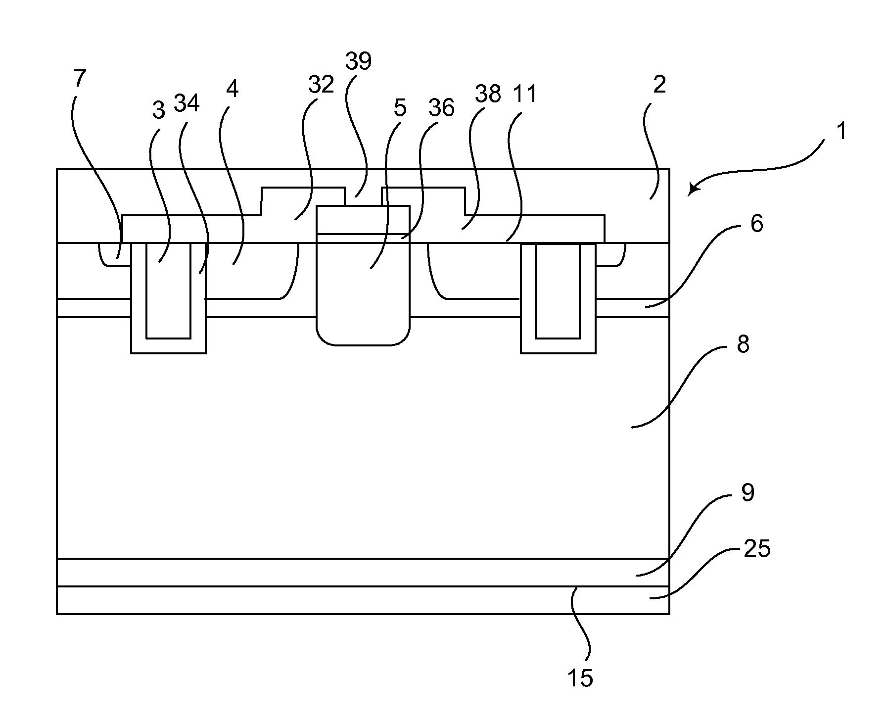
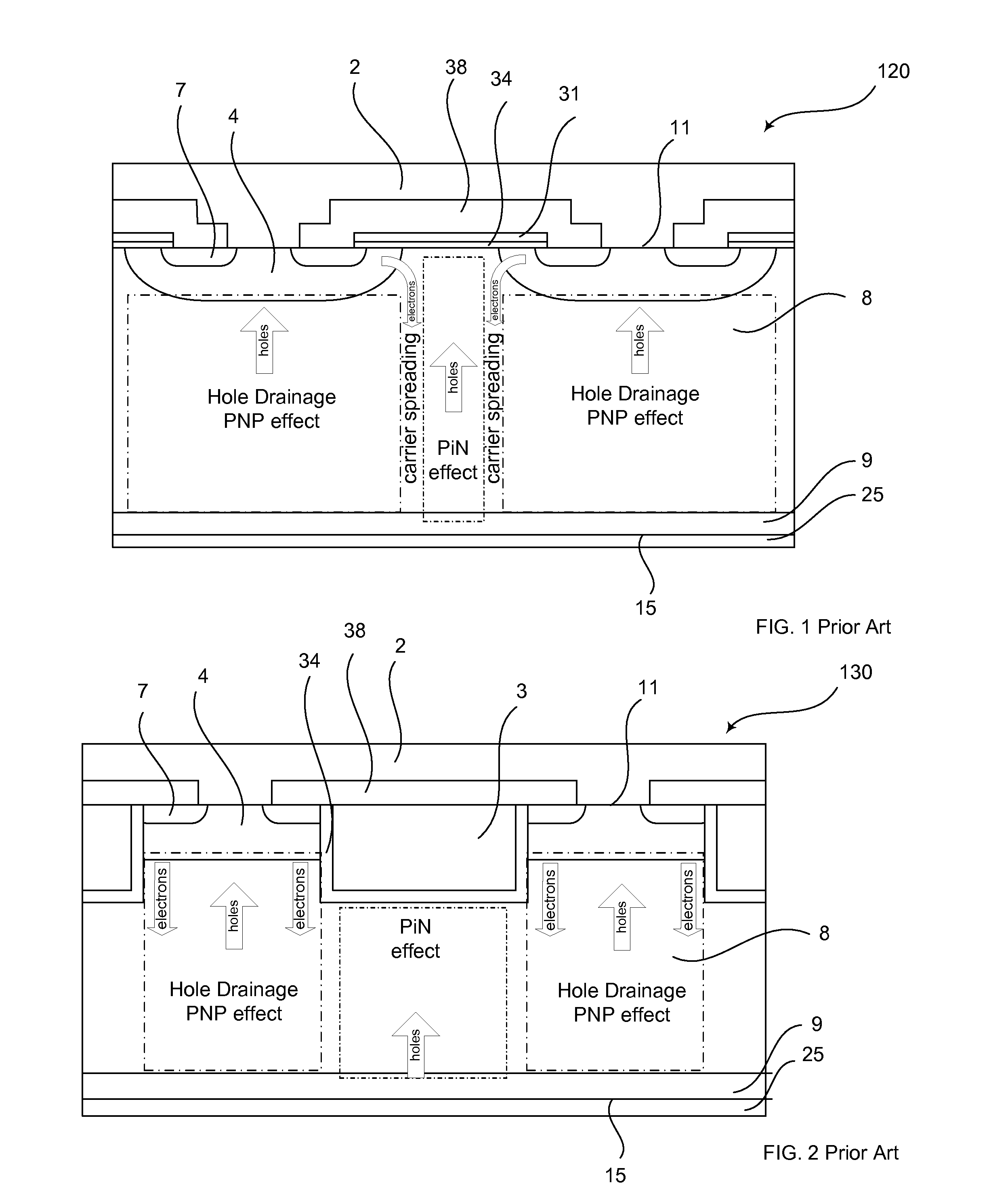
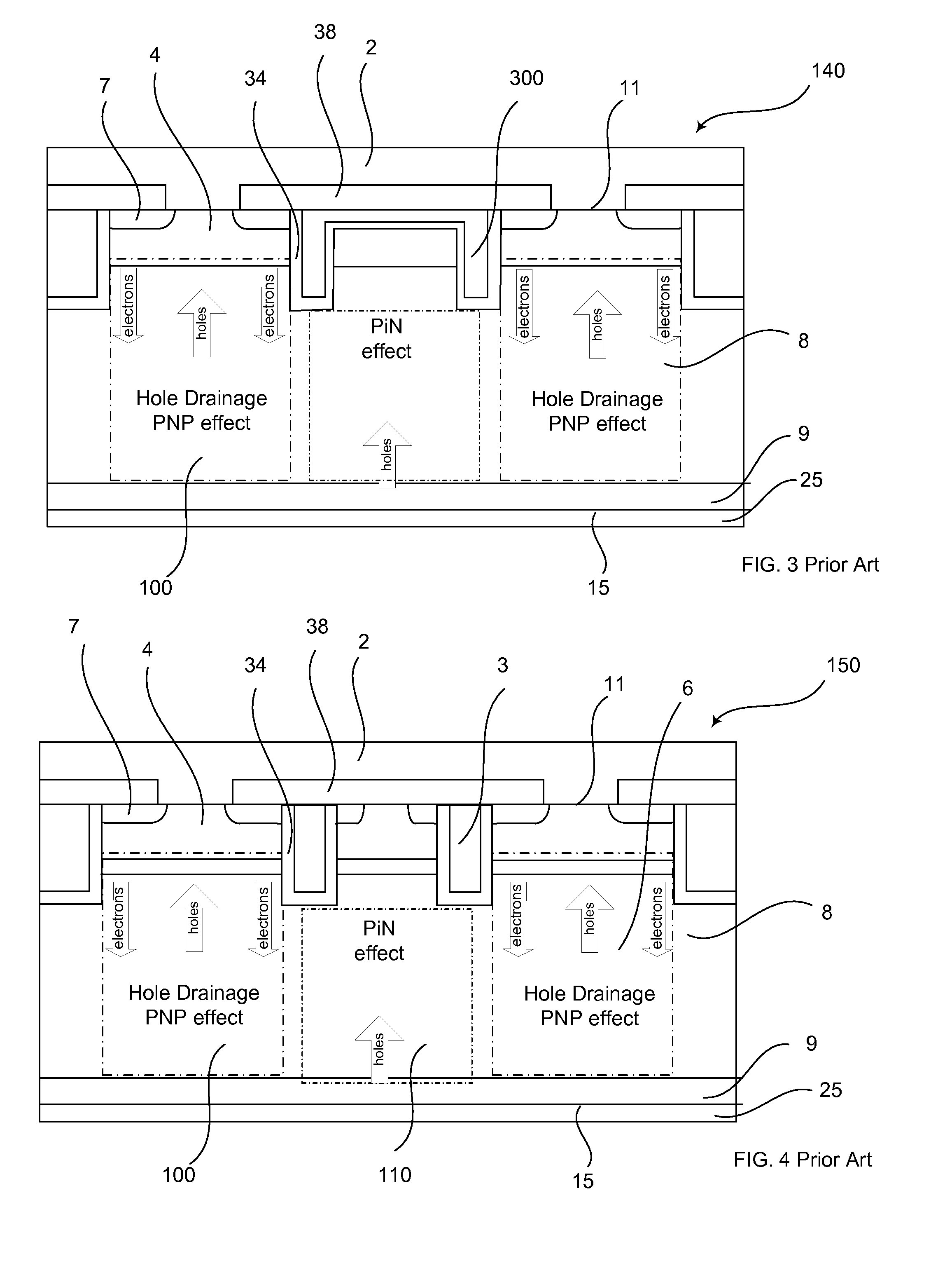
[0028]Exemplary embodiments of the present disclosure provide a power semiconductor device, such as an insulated gated bipolar transistor (IGBT), with reduced on-state losses, improved blocking capability, low drainage of holes and good controllability, which is easier to manufacture than known devices.

[0029]According to an exemplary embodiment, the IGBT has layers between an emitter electrode on an emitter side and a collector electrode on a collector side opposite to the emitter side. The IGBT includes a drift layer of a first conductivity type, and a collector layer of a second conductivity type different than the first conductivity type, where the collector layer is arranged between the drift layer and the collector electrode, and electrically contacts the collector electrode. The IGBT also includes a base layer of a second conductivity type, which is arranged between the drift layer and the emitter electrode, where the base layer is in direct electrical contact with the emitter...


PUM


Abstract

An IGBT has layers between emitter and collector sides. The layers include a collector layer on the collector side, a drift layer, a base layer of a second conductivity type, a first source region arranged on the base layer towards the emitter side, a trench gate electrode arranged lateral to the base layer and extending deeper into the drift layer than the base layer, a well arranged lateral to the base layer and extending deeper into the drift layer than the base layer, an enhancement layer surrounding the base layer so as to completely separate the base layer from the drift layer and the well, an electrically conducting layer covering the well and separated from the well by a second electrically insulating layer, and a third insulating layer having a recess on top of the electrically conducting layer such that the electrically conducting layer electrically contacts a emitter electrode.

Description

RELATED APPLICATIONS[0001]This application claims priority as a continuation application under 35 U.S.C. §120 to PCT / EP2012 / 063303, which was filed as an International Application on Jul. 6, 2012 designating the U.S., and which claims priority to European Application 11173059.4 filed in Europe on Jul. 7, 2011. The entire contents of these applications are hereby incorporated by reference in their entireties.FIELD[0002]The present disclosure relates to the field of power semiconductor devices. More particularly, the present disclosure relates to an Insulated Gate Bipolar Transistor (IGBT).BACKGROUND INFORMATION[0003]FIG. 1 shows a known IGBT 120 with planar gate electrodes. The IGBT 120 is a device with a four-layer structure, which layers are arranged between an emitter electrode 2 on an emitter side 11 and a collector electrode 25 on a collector side 15, which is arranged opposite of the emitter side 11. An (n−) doped drift layer 8 is arranged between the emitter side 11 and the co...

Claims


Application Information

Patent Timeline
Patent Type & Authority Applications(United States)
IPC IPC(8): H01L29/739H01L29/66
CPCH01L29/66348H01L29/7397H01L29/1095H01L29/7395H01L29/0619
Inventor ANDENNA, MAXIRAHIMO, MUNAFCORVASCE, CHIARAKOPTA, ARNOST
Owner HITACHI ENERGY SWITZERLAND AG
Why Eureka
Try Eureka