
Integrated optics logic gate for polarization-encoded quantum qubits and a method for the production and use thereof

a logic gate and optics technology, applied in logic circuits, quantum computers, computing models, etc., can solve the problems of increasing the complexity of optical systems, prohibiting the use of a large number of qubits, and working with bulk devices, so as to increase the complexity of production and the dimensions of devices, reduce the manufacturing yield, and increase the cost and dimension

Inactive Publication Date: 2014-05-08
CONSIGLIO NAT DELLE RICERCHE +1
View PDF4 Cites 29 Cited by
  • Summary
  • Abstract
  • Description
  • Claims
  • Application Information

AI Technical Summary

Benefits of technology

The present invention relates to a logic gate that can create entanglement or separate two qubits. The invention provides a waveguide that is necessary for the proper operation of the quantum logic gate. The technical effect of the invention is that it provides a reliable and effective way to operate quantum logic gates with high efficiency.

Problems solved by technology

The development of the possibility of manipulating the quantum information, in other words the qubits as defined above, represents a major technological challenge, since it requires the capacity to control in a highly precise way the propagation and interference of photons by means of which the information is encoded.
The complexity of optical systems increases with the number of qubits used, to the point that their use with a large number of qubits becomes prohibitive.
However, working with bulk devices has a number of drawbacks.
This requirement is unattainable with the experimental approaches used up to the present time.
This is because the development of increasingly complex quantum optical systems implemented in bulk optics suffers from serious limitations in terms of the stability, the operating accuracy and the physical dimensions of the equipment.
These requirements make it difficult to achieve high precision of measurement and impossible to produce (or transport) quantum optical components outside the laboratory in an industrial setting.
No systematic study has yet been made of the optical properties of waveguides in relation to the propagation and manipulation of polarization-encoded qubits with these structures.

Method used


Image

  • Integrated optics logic gate for polarization-encoded quantum qubits and a method for the production and use thereof
  • Integrated optics logic gate for polarization-encoded quantum qubits and a method for the production and use thereof
  • Integrated optics logic gate for polarization-encoded quantum qubits and a method for the production and use thereof

Examples


example

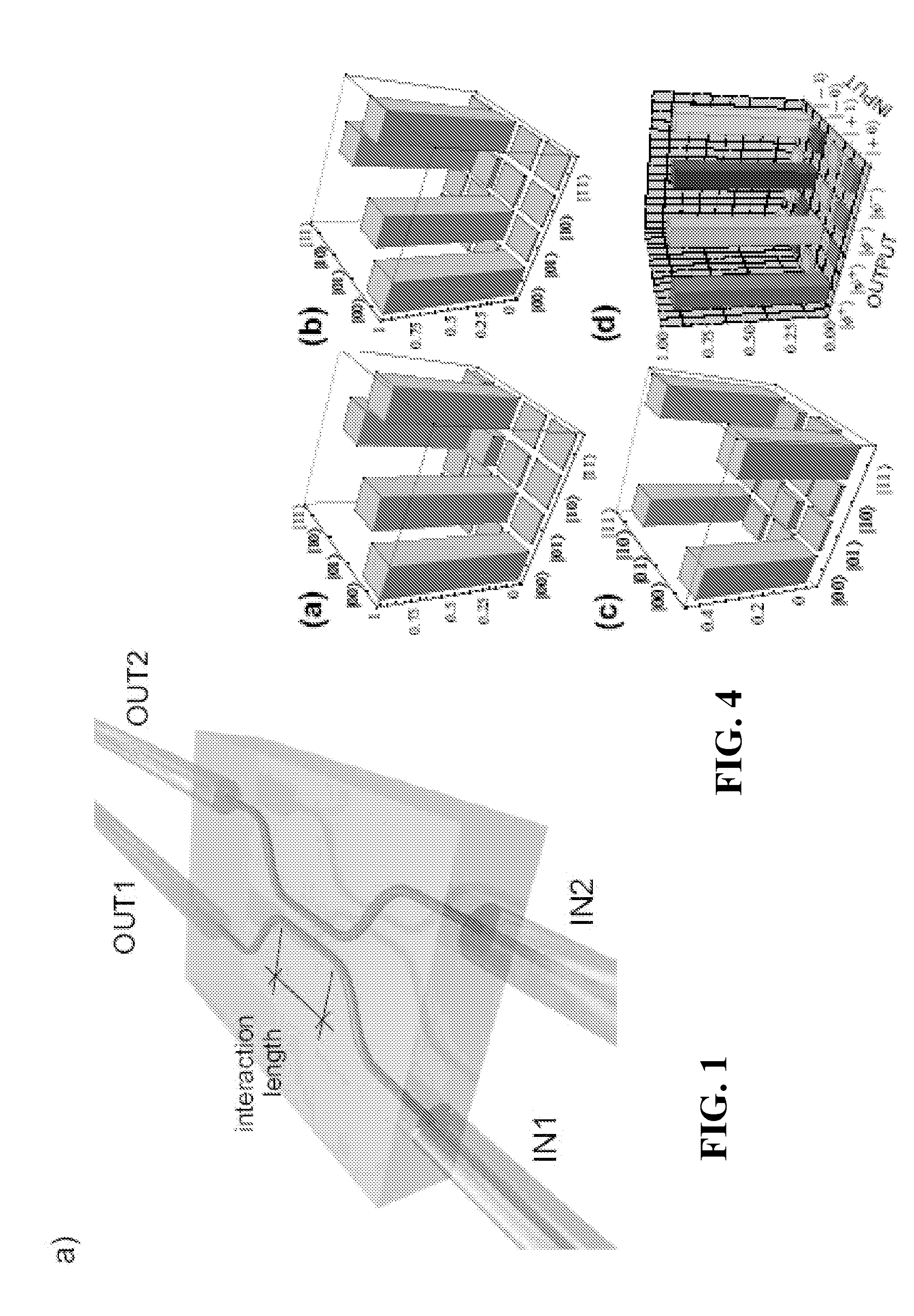
[0128]The apparatus of FIG. 3 can be divided into three sections. The first of these is a source of pairs of photons at a wavelength λ=808 nm, using “spontaneous parametric down conversion” in a β-barium borate crystal (C) with dimensions of 1.5 mm cut by non-linear “phase-matching”. The crystal was pumped with a laser diode having a power P=50 mW. The polarization states of the photons were prepared by using polarizing beam splitters (PBSs) and waveplates (WPs). A delay line (DL) was inserted to control the temporal superposition of the photons, which were then coupled to single mode fibres (SMFs) and injected into the integrated CNOT logic gate. Interference filters (IF) determine the bandwidth of the photons: Δλ=6 nm.

[0129]The logic gate is shown in detail in the insert and is described above.

[0130]The apparatus for analyzing the polarization of the qubits emerging from the CNOT gate is standard (WP+PBS). The photons were then sent to a single photon counting module (SPCM) throug...


PUM

PropertyMeasurementUnit
refractive indexaaaaaaaaaa
lengthaaaaaaaaaa

Abstract

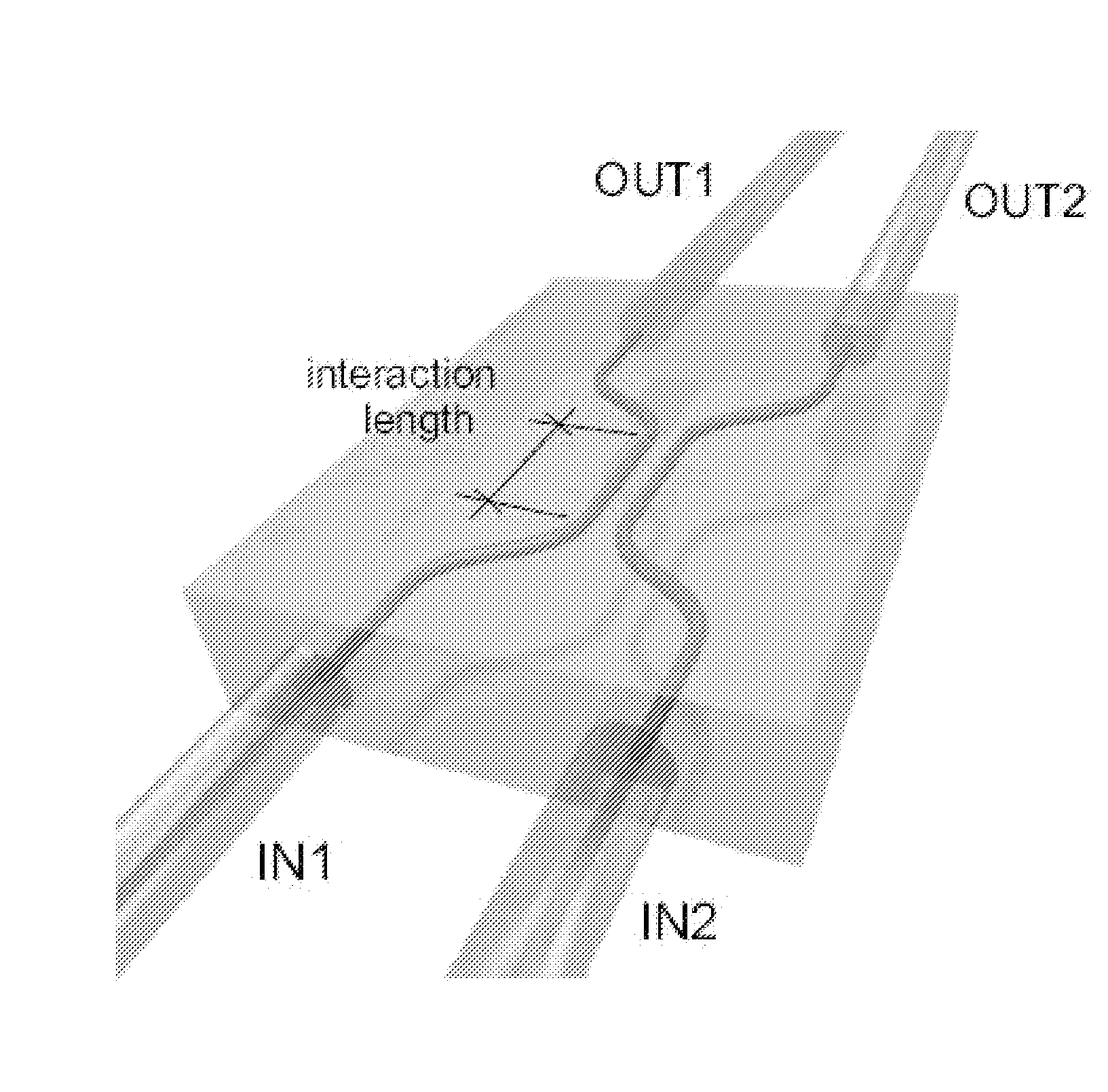
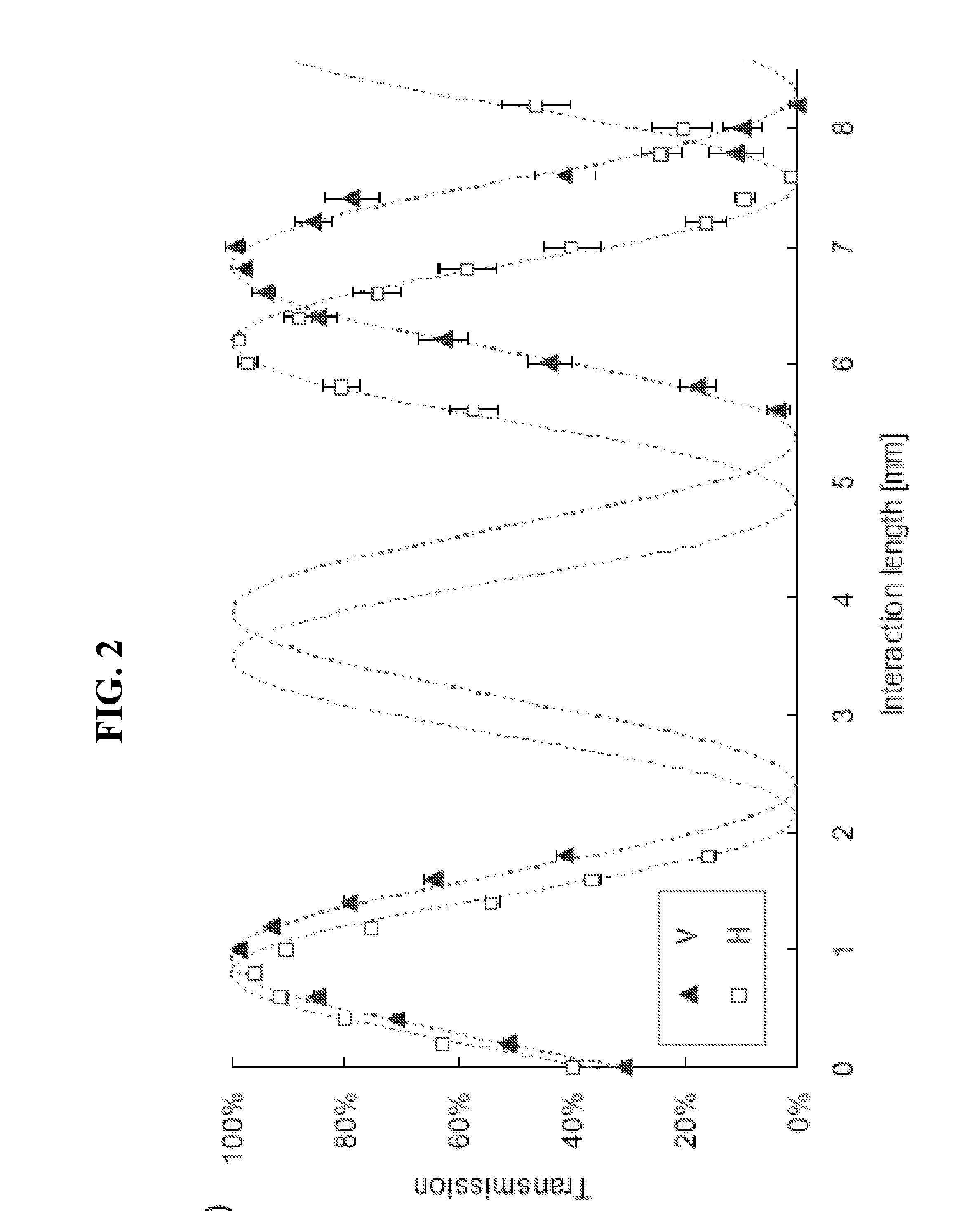
A quantum logic gate for qubits, suitable for receiving as inputs at least two polarization-encoded qubits, includes at least one partially polarizing beam splitter (PPBS), the beam splitter comprising a first waveguide and a second waveguide which are constructed in integrated optics, the first and second waveguides having a refractive index contrast of between 0.1% and 6% and a birefringence of between 10−6 and 6*10−5.

Description

TECHNICAL FIELD[0001]The present invention relates to a quantum logic gate for at least two qubits encoded in the polarization of single photons and a method for the production and use of a quantum logic gate, the gate comprising an integrated device having the structure of a partially polarizing beam splitter including at least two birefringent waveguides, whose behaviour is dependent on the polarization of the photons sent as inputs.PRIOR ART[0002]The use of the laws of quantum mechanics for storing, manipulating and transmitting data is very likely to lead, in the near future, to a major advance in the resolution of a number of complex problems in computing which cannot be tackled with existing technology. The production of a quantum computer is an objective viewed with increasing interest in the scientific community. Quantum cryptographic methods are also used in devices available on the market, such as the product known as MagiQ QPN Security Gateway (QPN-8505) and those produce...

Claims


Application Information

Patent Timeline
Patent Type & Authority Applications(United States)
IPC IPC(8): G02F3/00G06N99/00
CPCG06N99/002G02F3/00B82Y10/00G02B6/126G02B6/274G02B2006/12038G02B2006/12147G02B2006/1215G02B2006/12171G06N10/00
Inventor CRESPI, ANDREAMATALONI, PAOLORAMPONI, ROBERTASANSONI, LINDASCIARRINO, FABIOVALLONE, GIUSEPPEOSELLAME, ROBERTO
Owner CONSIGLIO NAT DELLE RICERCHE
Learn More