Plasma etching method and plasma etching apparatus

a plasma etching and plasma technology, applied in the direction of electrical equipment, basic electric elements, electric discharge tubes, etc., can solve the problems of etching lines that may be wiped, lines formed by etching may be roughened, and the cross-sectional shape of lines may be deteriorated, so as to reduce the roughness of lines formed and improve the cross-sectional shape of lines

Active Publication Date: 2014-05-15
TOKYO ELECTRON LTD
View PDF2 Cites 188 Cited by
  • Summary
  • Abstract
  • Description
  • Claims
  • Application Information

AI Technical Summary

Benefits of technology

[0007]According to various aspects and embodiments of the present invention, a plasma etching apparatus and a plasma etching method capable of reducing the roughness of the lines formed by etching and improving the cross-sectional shape of the lines are realized.

Problems solved by technology

However, in the conventional technique, since the roughness of the amorphous carbon film due to etching is transferred to the underlying silicon oxide film, the lines formed by etching may be roughened, or the cross-sectional shape of the lines may be deteriorated.
Meanwhile, in the conventional technique, when etching the silicon oxide film while supplying a high frequency bias power, wiggling of lines formed by etching may occur.

Method used


Image

  • Plasma etching method and plasma etching apparatus
  • Plasma etching method and plasma etching apparatus
  • Plasma etching method and plasma etching apparatus

Examples


example 1

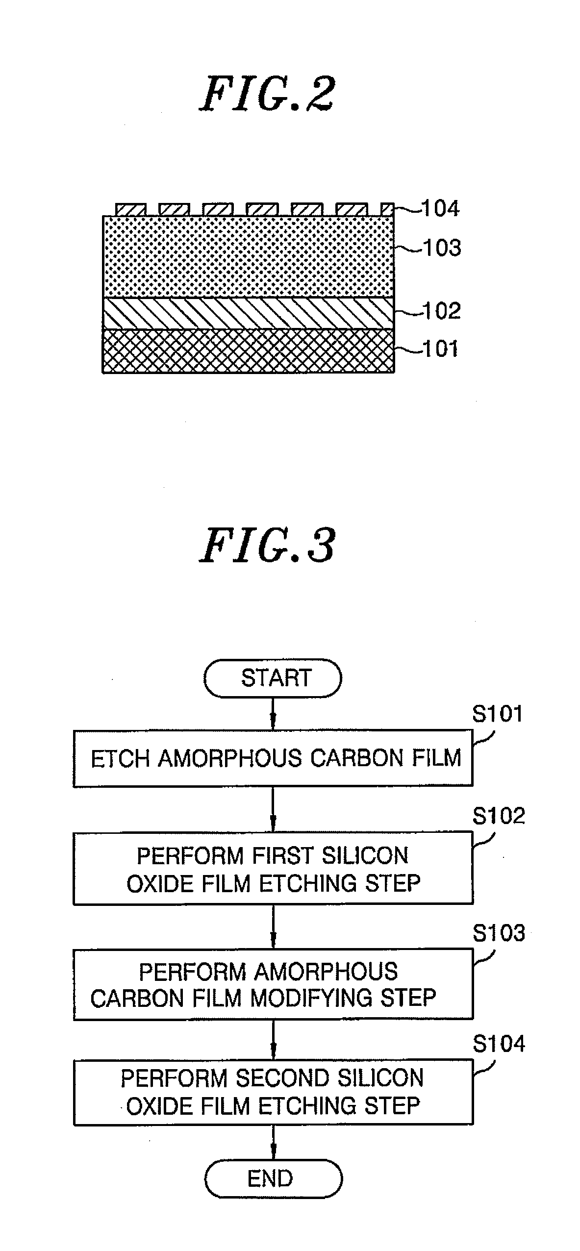
[0082]In Example 1, after an amorphous carbon film etching step and a first silicon oxide film etching step were sequentially performed on a target object, an amorphous carbon film modifying step of modifying an amorphous carbon film was performed, and then, a second silicon oxide film etching step was performed. The amorphous carbon film etching step, the first silicon oxide film etching step and the second silicon oxide film etching step were carried out under the same conditions as in Comparative Example 1. The amorphous carbon film modifying step was performed under the following conditions.

[0083](Amorphous Carbon Film Modifying Step)

[0084]Processing gas flow ratio: COS / CF4 / Ar=20:30:800

[0085]Pressure: 6.7 Pa (50 mTorr)

[0086]High frequency power from the first high frequency power supply: 300 W

[0087]High frequency power from the second high frequency power supply: 0 W

[0088]DC voltage to the upper electrode: −900 V

Example 2

[0089]In the amorphous carbon film modifying step, a proce...

example 2

H2 / Ar=100:800

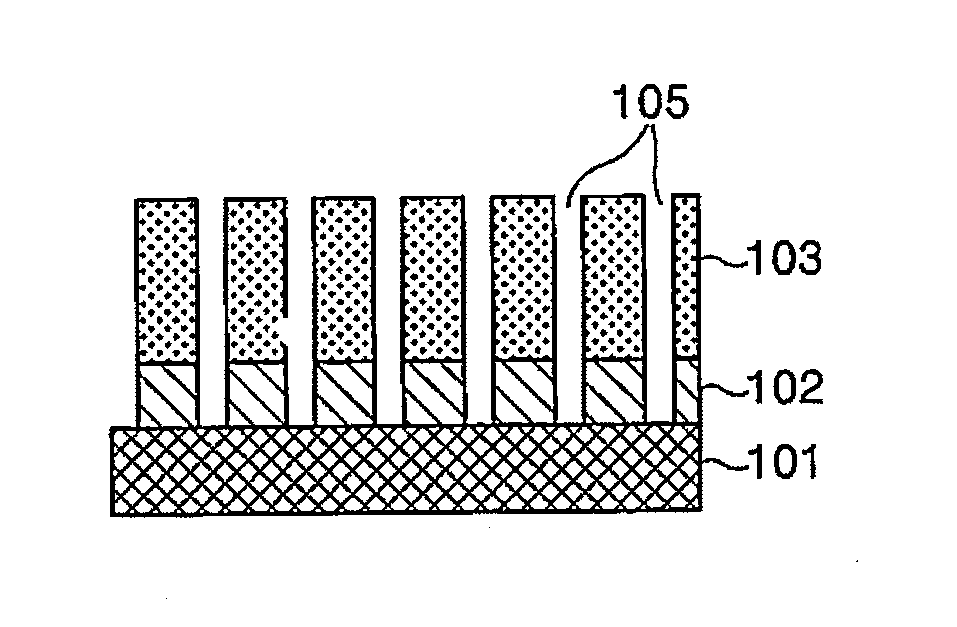
[0090]FIGS. 5 and 6 are diagrams showing the processing results in Comparative Example 1, Example 1 and Example 2. In FIG. 5, “Post ME1” indicates the target object after performing the first silicon oxide film etching step in Comparative Example 1 and Example 1. Further, “COS / CF4 / Ar Hardening” indicates the target object after performing the second silicon oxide film etching step in Example 1, and “H2 / Ar Hardening” indicates the target object after performing the second silicon oxide film etching step in Example 2. Furthermore, “w / o Hardening” refers to the target object after performing the second silicon oxide film etching step in Comparative Example 1. In FIG. 5, “cross-section” and “upper surface” are trace diagrams of photographs obtained by expanding the cross-section and the upper surface of the target object, respectively.

[0091]Further, FIGS. 5 and 6 show line width roughness (LWR), space width roughness (SWR), line edge roughness (LER) and “Sum” that is the su...


PUM

PropertyMeasurementUnit
frequencyaaaaaaaaaa
frequencyaaaaaaaaaa
DC voltageaaaaaaaaaa

Abstract

A plasma etching method includes etching an amorphous carbon film by a plasma of an oxygen-containing gas using, as a mask, an SiON film having a predetermined pattern formed on a target object, etching a silicon oxide film by a plasma of a processing gas using the amorphous carbon film as a mask while removing the SiON film remaining on the etched amorphous carbon film by the plasma of the processing gas. The plasma etching method further includes modifying the amorphous carbon film by a plasma of a sulfur-containing gas or a hydrogen-containing gas while applying a negative DC voltage to an upper electrode containing silicon after the SiON film is removed from the amorphous carbon film, and etching the silicon oxide film again by the plasma of the processing gas using the modified amorphous carbon film as a mask.

Description

CROSS-REFERENCE TO RELATED APPLICATION[0001]This application claims priority to Japanese Patent Application No. 2012-247781, filed on Nov. 9, 2012 and U.S. Provisional Application No. 61 / 727,194, filed on Nov. 16, 2012, the entire contents of which are incorporated herein by reference.FIELD OF THE INVENTION[0002]Embodiments and aspects of the present invention relate to a plasma etching method and a plasma etching apparatus.BACKGROUND OF THE INVENTION[0003]Conventionally, a technique for etching a multilayer film formed on a target object has been known. For example, there is disclosed a technique of etching an amorphous carbon film by a plasma of a sulfur-containing gas using, as a mask, an SiON film having a predetermined pattern formed on the target object, and etching a silicon oxide film by a plasma of a CF-based gas using the amorphous carbon film as a mask (see, e.g., Japanese Patent Application Publication No. 2011-216644).[0004]However, in the conventional technique, since ...

Claims


Application Information

Patent Timeline
Patent Type & Authority Applications(United States)
IPC IPC(8): H01L21/311
CPCH01L21/31144H01L21/31116H01J2237/334H01L21/3105H01L21/31122
Inventor SEYA, YUTA
Owner TOKYO ELECTRON LTD
Why Eureka
Try Eureka