Method and apparatus for dynamic current distribution control during electroplating

a dynamic current and electroplating technology, applied in the direction of manufacturing tools, electric circuits, electric circuits, etc., can solve the problems of increasing the difficulty of controlling the terminal effect, increasing the difficulty of achieving uniform initial plating across the wafer, and increasing the difficulty of achieving uniform initial plating.

Active Publication Date: 2014-05-29
LAM RES CORP
View PDF10 Cites 28 Cited by
  • Summary
  • Abstract
  • Description
  • Claims
  • Application Information

AI Technical Summary

Benefits of technology

[0006]The difficulty in controlling the terminal effect is further exacerbated by the fact that it is very pronounced in the beginning of electroplating when the seed layer on the wafer is most resistive, but is rapidly diminishing during the course of electroplating. As electroplating proceeds, the plated layer becomes thicker and ...

Problems solved by technology

It becomes a very challenging problem to achieve uniform initial plating across the wafer with such resistive seed layers.
Without appropriate means of resistance and voltage compensation, this large edge-to-center voltage drop could lead to an extremely non-uniform plating thickness distribution, primarily characterized by thicker plating at the wafer edge.
The...

Method used


Image

  • Method and apparatus for dynamic current distribution control during electroplating
  • Method and apparatus for dynamic current distribution control during electroplating
  • Method and apparatus for dynamic current distribution control during electroplating

Examples


Embodiment Construction

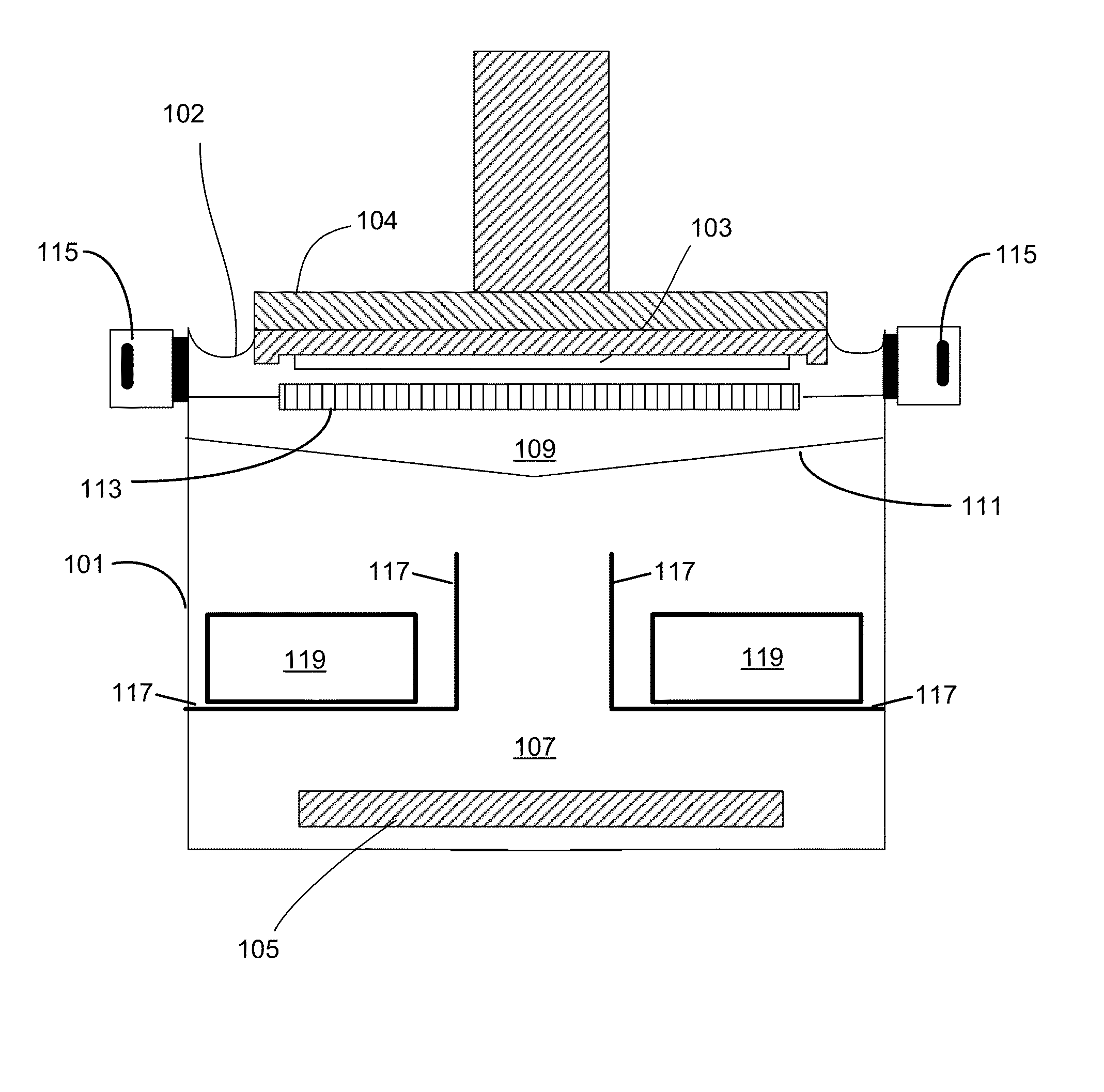
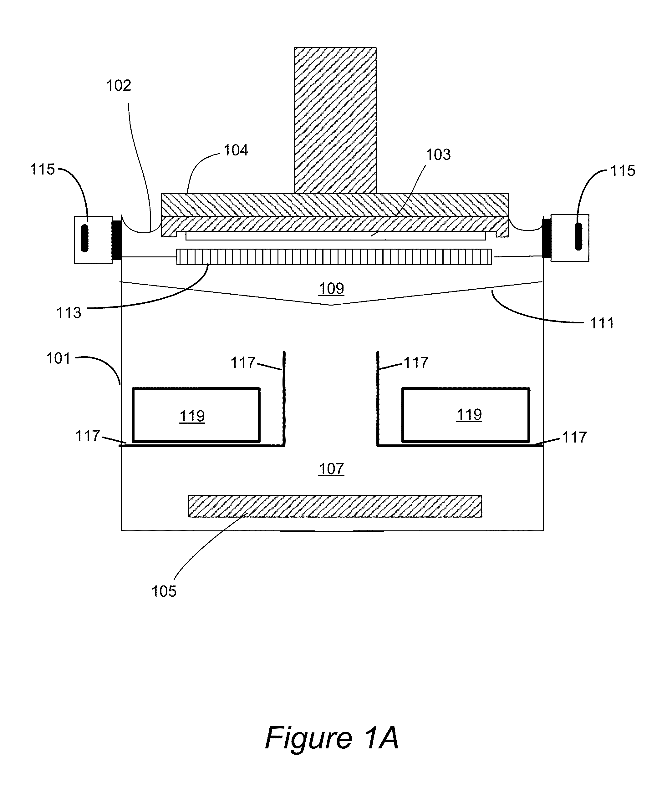
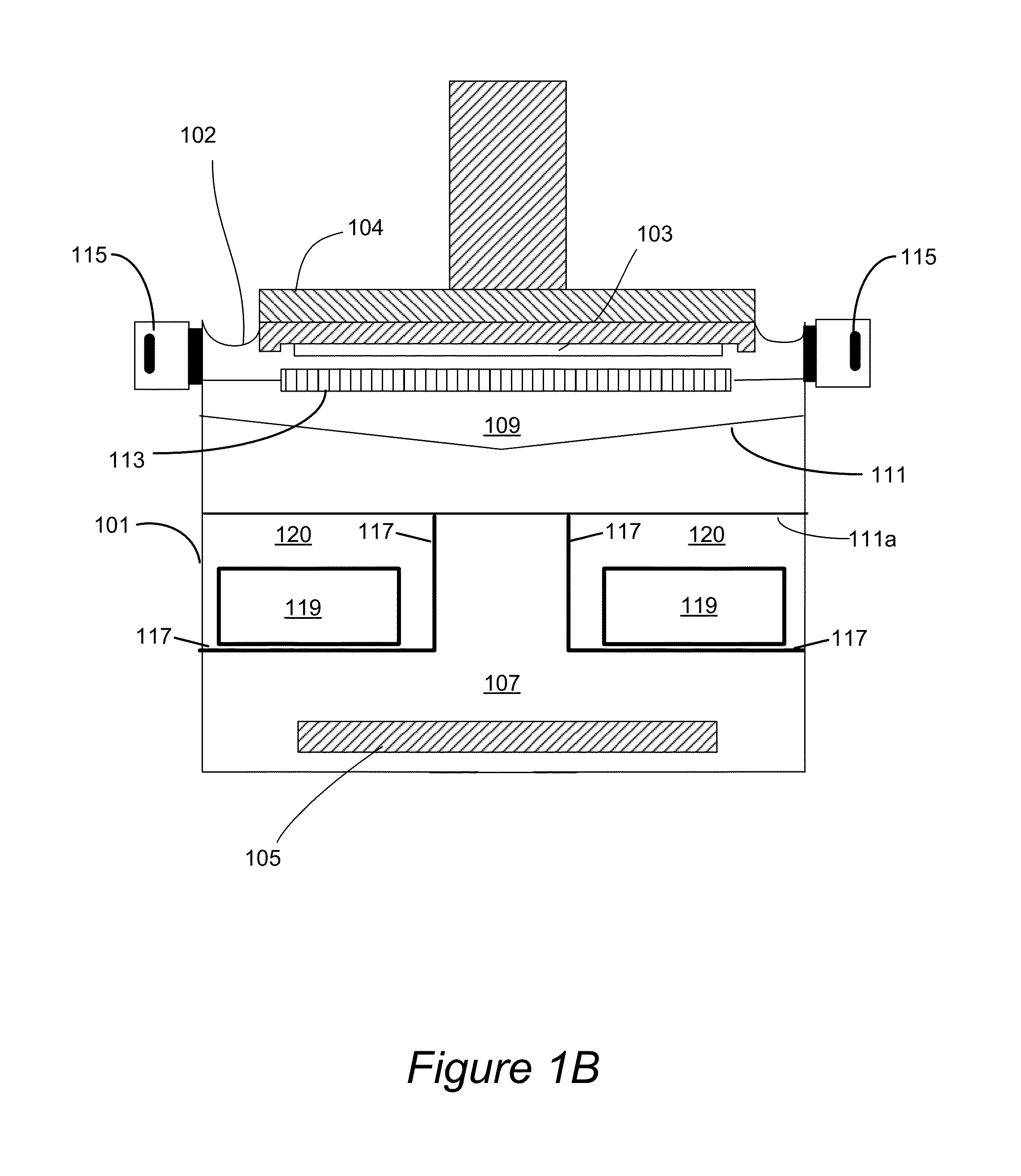
[0027]The methods and apparatus provided herein are useful for electroplating a variety of metals including but not limited to copper and its alloys on semiconductor substrates having one or more recessed features (e.g., trenches and vias). The methods and apparatus are useful for electroplating on 300 mm and, particularly, on 450 mm semiconductor wafers and on resistive seed layers. For example, the apparatus and methods, can be used, in some embodiments, for electroplating on seed layers having seed sheet resistance of up to about 50 Ohm / sq. (inclusive of this number), e.g. with sheet resistance of between about 10-50 Ohm / sq., such as between about 20-40 Ohm / sq. Examples of substrates that can be processed by provided methods include, without limitation, a 300 mm wafer having a copper seed layer having a thickness of between about 10-2000 Å, or a 450 mm wafer having a copper seed layer having a thickness of between about 20-2000 Å. In some embodiments the initial copper seed layer...


PUM

PropertyMeasurementUnit
Fractionaaaaaaaaaa
Thicknessaaaaaaaaaa
Fractionaaaaaaaaaa

Abstract

An apparatus for electroplating a layer of metal onto the surface of a wafer includes an auxiliary electrode that is configured to function both as an auxiliary cathode and an auxiliary anode during the course of electroplating. The apparatus further includes an ionic current collimator (e.g., a focus ring) configured to direct ionic current from the main anode to central portions of the wafer. The provided configuration effectively redistributes ionic current in the plating system allowing plating of uniform metal layers and mitigating the terminal effect. In one example, the auxiliary electrode functions as an auxiliary cathode in the beginning of electroplating when the terminal effect is pronounced, and subsequently is anodically biased.

Description

CROSS-REFERENCE TO RELATED APPLICATIONS[0001]This application claims benefit of prior U.S. Provisional Application No. 61 / 730,285 filed Nov. 27, 2012, titled “Method and Apparatus for dynamic Current Distribution Control during Electroplating” naming Zhian He as the inventor, which is herein incorporated by reference in its entirety and for all purposes.FIELD OF THE INVENTION[0002]The present invention pertains to methods and apparatuses for electroplating. Specifically, the invention pertains to electroplating tools used for electrodeposition of metals in semiconductor processing.BACKGROUND OF THE INVENTION[0003]The transition from aluminum to copper in integrated circuit (IC) fabrication required a change in process “architecture” (to damascene and dual-damascene) as well as a whole new set of process technologies. One process step used in producing copper damascene circuits is the formation of a “seed-” or “strike-” layer, which is then used as a base layer onto which copper is e...

Claims


Application Information

Patent Timeline
IPC IPC(8): C25D17/00H01L21/02
CPCC25D5/022C25D17/001C25D17/002C25D17/007C25D17/008C25D17/10C25D21/12H01L21/2885C25D7/123
Inventor HE, ZHIAN
Owner LAM RES CORP
Why Eureka
Try Eureka