Solid-state image sensor, and imaging system

a solid-state image sensor and imaging system technology, applied in the direction of instruments, radiation controlled devices, optical radiation measurement, etc., can solve the problem of the energy of the light being spatially separated in the wavelength direction, the energy resolution of the wavelength is not matched with respect, etc. problem, to achieve the effect of high spatial resolution, high wavelength resolution and high sensitivity

Active Publication Date: 2014-05-29
SONY CORP
View PDF9 Cites 42 Cited by
  • Summary
  • Abstract
  • Description
  • Claims
  • Application Information

AI Technical Summary

Benefits of technology

[0039]According to the present invention, a spectroscopic/imaging device for visible/near-infrared light having a high sensitivity

Problems solved by technology

However, there is no energy resolution (wavelength resolution) with respect to an electromagnetic wave with wavelength shorter than 1.1 μm, and it is difficult to identify light of which wavelength is detected based on the accumulated charge.
As an inevitable issue in the case of dispersing light by a grating, there is an issue of the energy of the light being spatially separated in the wavelength direction.
Furthermore, there is also an issue that, since the incident light has to be transmitted through a narrow slit, the amount of light entering the sensor is small in the first place.
In the case of the method above of arranging several types of filters

Method used


Image

  • Solid-state image sensor, and imaging system
  • Solid-state image sensor, and imaging system
  • Solid-state image sensor, and imaging system

Examples


Embodiment Construction

[0056]Hereinafter, an embodiment of the present invention will be described in association with the drawings.

[0057]Moreover, description will be given in the following order.

1. Example Schematic Configuration of Entire CMOS Solid-State Image Sensor

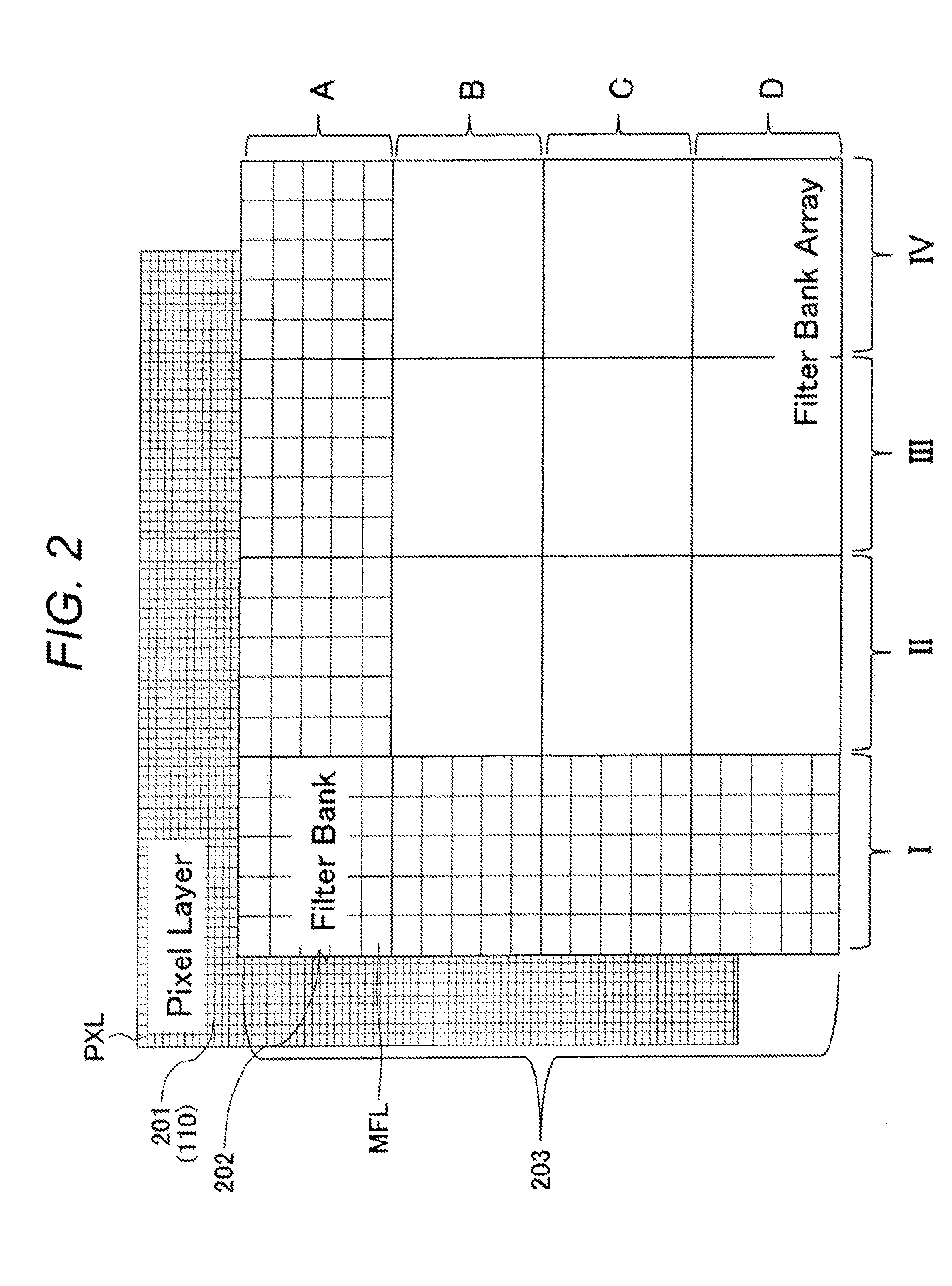
2. Positional Relationship of Solid-State Image Sensor and Metal Thin Film Filter

3. Example Configuration of Metal Film Filter

[0058]4. Example Structure of Solid-State Image Sensor where Metal Thin Film Filter is Arranged

5. Method of Estimating Electromagnetic Spectrum Waveform of Subject

6. Example Configuration of Spectroscopic Imaging System

7. Manufacturing Method of Metal Thin Film Filter

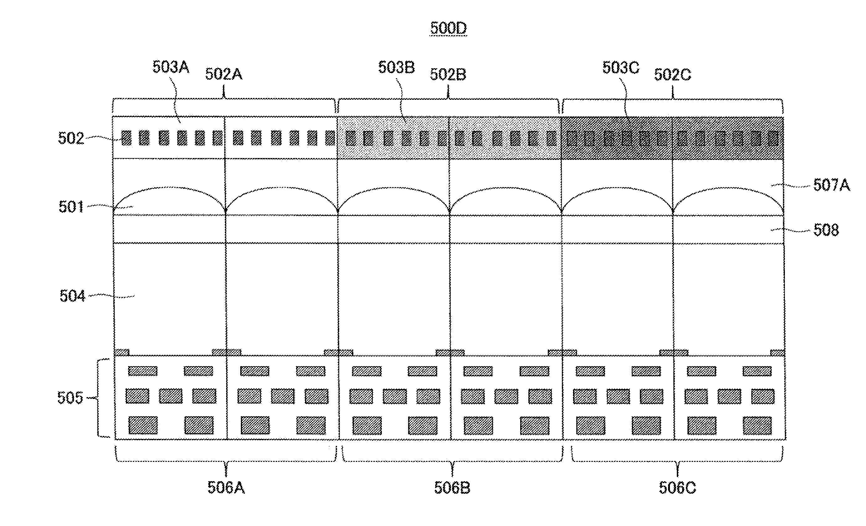
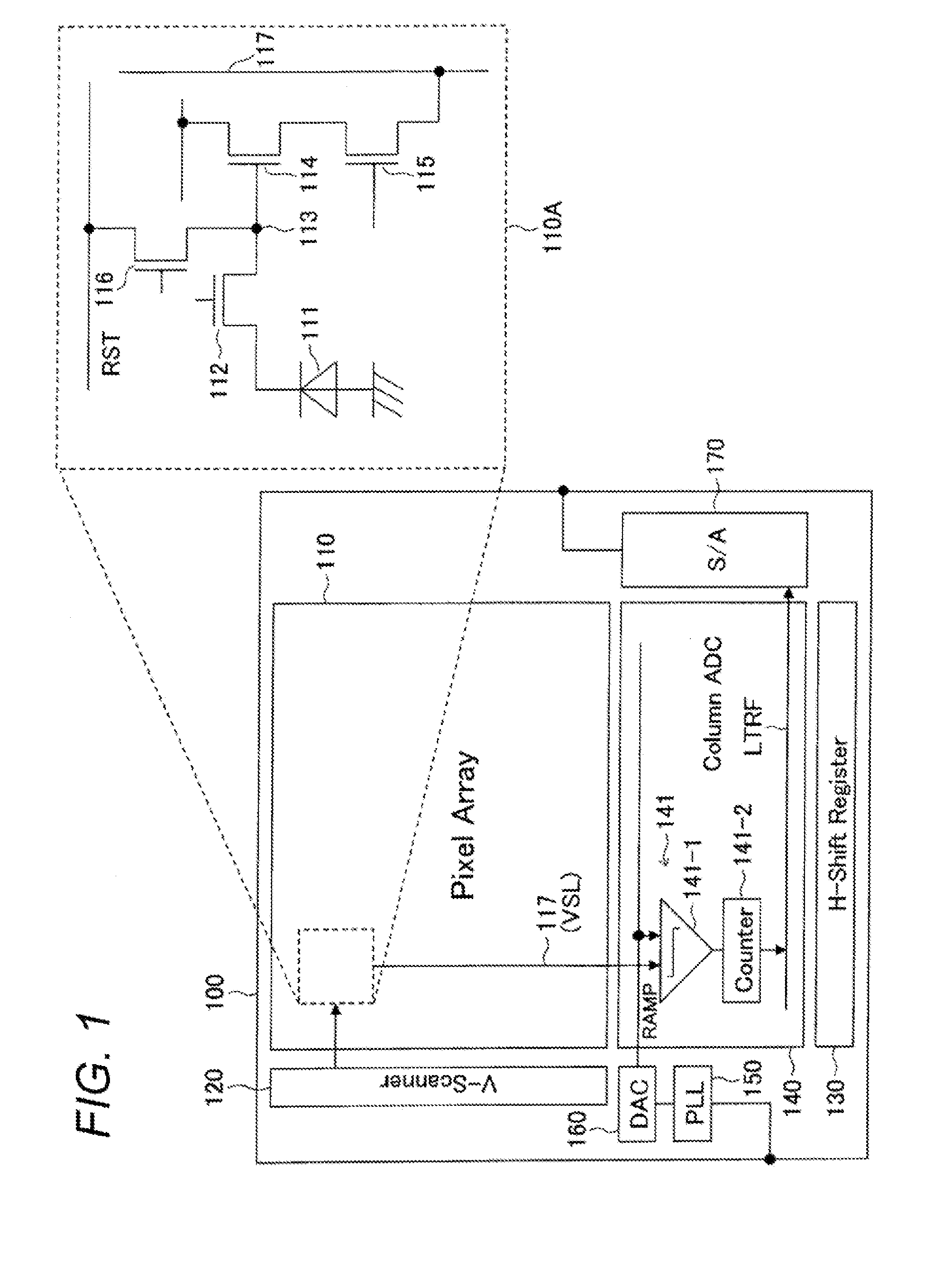
[0059]FIG. 1 is a block diagram showing an example configuration of a CMOS solid-state image sensor according to the present embodiment.

[0060]In the following, an example is described where a metal filter of the present technology is mounted on a backside illumination CMOS solid-state image sensor. Additionally, it is needless to say that application to...


PUM


Abstract

The present technology relates to solid-state image sensor and an imaging system which are capable of providing a solid-state image sensor and an imaging system which are capable of realizing a spectroscopic/imaging device for visible/near-infrared light having a high sensitivity and high wavelength resolution, and of achieving two-dimensional spectrum mapping with high spatial resolution. There are provided a two-dimensional pixel array, and a plurality of types of filters that are arranged facing a pixel region of the two-dimensional pixel array, the filters each including a spectrum function and a periodic fine pattern shorter than a wavelength to be detected, wherein each of the filters forms a unit which is larger than the photoelectric conversion device of each pixel on the two-dimensional pixel array, where one type of filter is arranged for a plurality of adjacent photoelectric conversion device groups, wherein the plurality of types of filters are arranged for adjacent unit groups to form a filter bank, and wherein the filter banks are arranged in a unit of N×M, where N and M are integers of one or more, facing the pixel region of the two-dimensional pixel array.

Description

TECHNICAL FIELD[0001]The present technology relates to a solid-state image sensor including a metal thin film filter having a periodic fine pattern shorter than a wavelength to be detected, and an imaging system.BACKGROUND ART[0002]A spectroscopic sensor is used for non-invasive examination in various fields such as medical treatment, cosmetic care, and health.[0003]A general spectroscopic sensor irradiates a subject with electromagnetic light from a visible light source, an infrared light source or the like, or by a laser, an LED or the like that radiates light at narrow band wavelength, and causes the reflected light or a light component shifted by Raman scattering to pass through a slit to be transmitted through / reflected by a grating. The spectroscopic sensor thereby converts a signal intensity distribution in the wavelength direction into a spatial signal intensity distribution.[0004]Then, an incident spectrum may be restored by detecting the electromagnetic wave intensity of e...

Claims


Application Information

Patent Timeline
IPC IPC(8): H01L27/146H04N9/07
CPCH04N9/07H01L27/14621G02B5/201H01L27/14629G02B5/008G01J3/12G01J3/18G01J3/2803G01J3/2823G01J2003/1213G01J2003/2806G01J2003/282G01J2003/2826G01J3/0259G01J3/027G01J2003/2816H04N23/11H04N23/12H04N25/76H04N25/75H01L27/14603
Inventor YOKOGAWA, SOZO
Owner SONY CORP
Why Eureka
Try Eureka