Recessed Channel Insulated-Gate Field Effect Transistor with Self-Aligned Gate and Increased Channel Length

a field effect transistor and self-aligning technology, applied in the field of integrated circuits, can solve the problems of undesired effects observed in the electrical characteristics of mos transistors, general undesirable subthreshold leakage in digital circuits, and large variance in leakage due to inwe, so as to achieve the effect of increasing the channel length

Active Publication Date: 2014-06-12
TEXAS INSTR INC
View PDF3 Cites 31 Cited by
  • Summary
  • Abstract
  • Description
  • Claims
  • Application Information

AI Technical Summary

Benefits of technology

[0013]Embodiments of this invention provide a transistor structure and method of fabricating t

Problems solved by technology

At these extremely small channel lengths, however, certain undesired effects in the electrical characteristics of MOS transistors have been observed.
This subthreshold leakage is generally undesirable in digital circuits, particularly in applications that are sensitive to power consumption, such as mobile devices, implantable medical devices, and other battery-powered systems.
Leakage due to INWE typically exhibits a relatively large variance over a population of transistors, particularly in devices in which the channel edges are not well-controlled.
This large variance is especially problematic in those analog circuits that rely on good matching of device c

Method used


Image

  • Recessed Channel Insulated-Gate Field Effect Transistor with Self-Aligned Gate and Increased Channel Length
  • Recessed Channel Insulated-Gate Field Effect Transistor with Self-Aligned Gate and Increased Channel Length
  • Recessed Channel Insulated-Gate Field Effect Transistor with Self-Aligned Gate and Increased Channel Length

Examples


Embodiment Construction

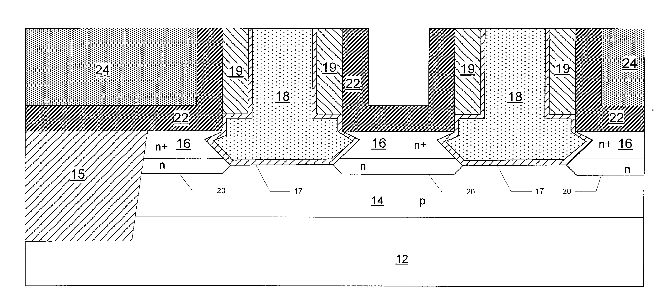
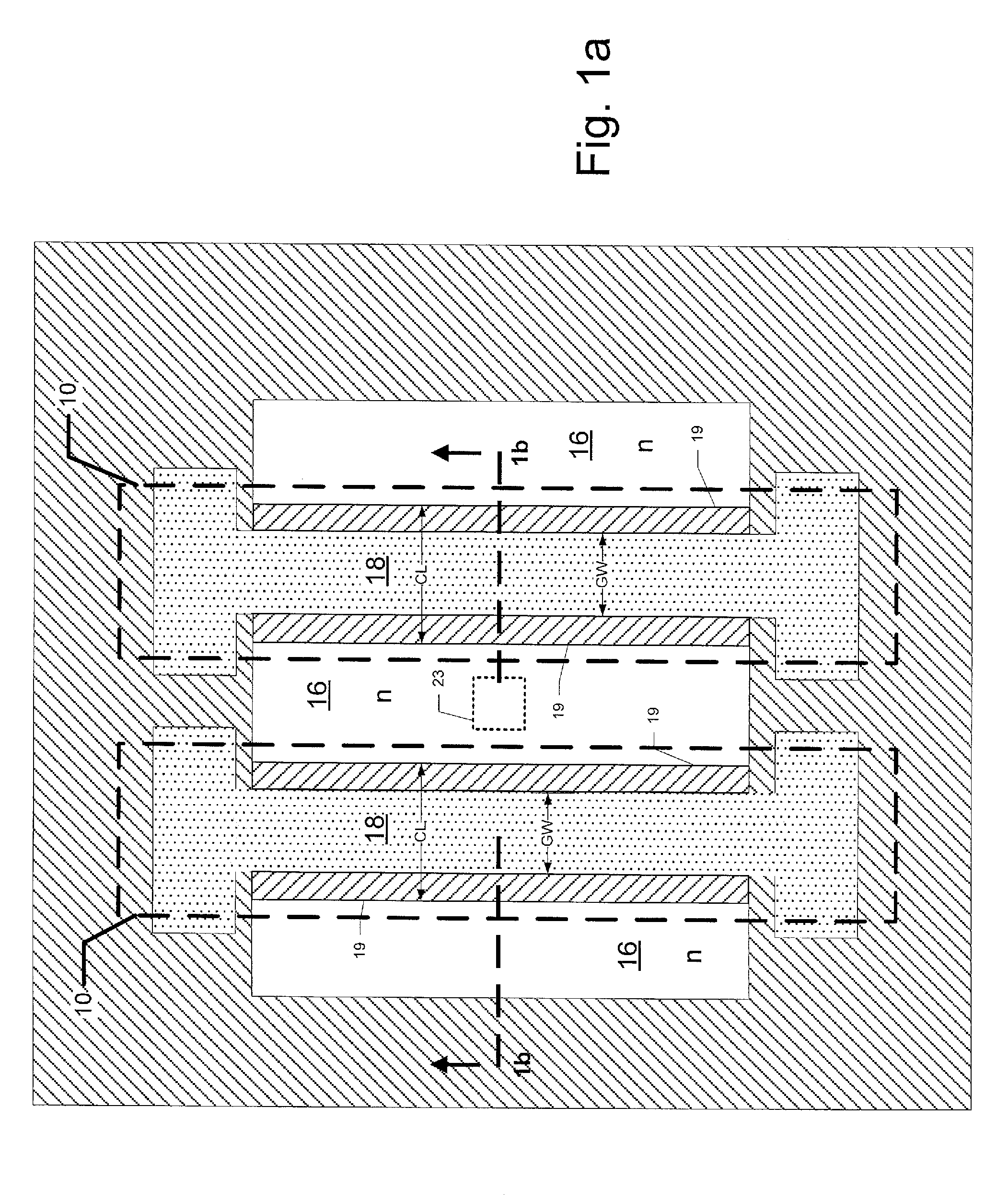
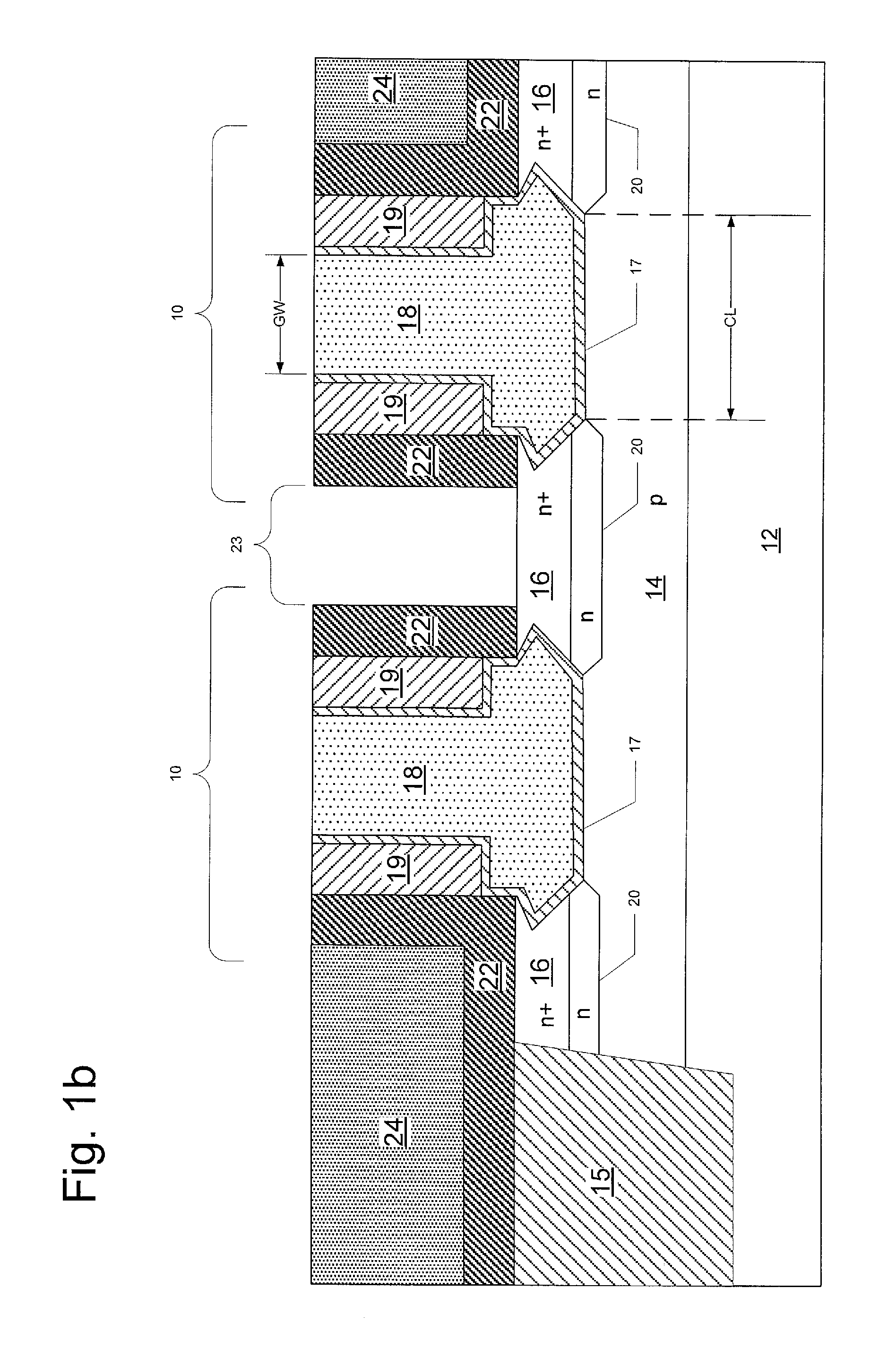
[0023]This invention will be described in connection with its embodiments, namely as implemented into an integrated circuit using a high-k gate dielectric and a gate material of a compatible metal, as it is contemplated that this invention will be especially beneficial when used in such an application. However, it is contemplated that embodiments of this invention will be beneficial when used in connection with other technologies and in other applications. Accordingly, it is to be understood that the following description is provided by way of example only, and is not intended to limit the true scope of this invention as claimed.

[0024]FIGS. 1a and 1b illustrate, in plan and cross-sectional views, respectively, of two instances of transistor 10 constructed according to embodiments of this invention. In this example, each transistor 10 is an metal-oxide semiconductor (MOS) transistor formed at a selected location of the surface of single-crystal silicon substrate 12. More specifically...


PUM


Abstract

A metal-oxide-semiconductor transistor (MOS) and method of fabricating the same, in which the effective channel length is increased relative to the width of the gate electrode. A dummy gate electrode overlying dummy gate dielectric material is formed at the surface of the structure, with self-aligned source/drain regions, and dielectric spacers on the sidewalls of the dummy gate structure. The dummy gate dielectric underlies the sidewall spacers. Following removal of the dummy gate electrode and the underlying dummy gate dielectric material, including from under the spacers, a silicon etch is performed to form a recess in the underlying substrate. This etch is self-limiting on the undercut sides, due to the crystal orientation, relative to the etch of the bottom of the recess. The gate dielectric and gate electrode material are then deposited into the remaining void, for example to form a high-k metal gate MOS transistor.

Description

CROSS-REFERENCE TO RELATED APPLICATIONS[0001]Not applicable.STATEMENT REGARDING FEDERALLY SPONSORED RESEARCH OR DEVELOPMENT[0002]Not applicable.BACKGROUND OF THE INVENTION[0003]This invention is in the field of integrated circuits and their manufacture. Embodiments of this invention are more particularly directed to metal-oxide-semiconductor field-effect transistors (MOSFETs) with extremely narrow gate electrodes.[0004]Many modern electronic devices and systems now include substantial computational capability for controlling and managing a wide range of functions and useful applications. As is fundamental in the art, reduction in the size of physical feature sizes of structures realizing transistors and other solid-state devices enables greater integration of more circuit functions per unit “chip” area, or conversely, reduced consumption of chip area for a given circuit function. The capability of integrated circuits for a given cost has greatly increased as a result of this miniatu...

Claims


Application Information

Patent Timeline
IPC IPC(8): H01L29/78H01L29/66
CPCH01L29/045H01L29/4236H01L29/42364H01L29/66545H01L29/66621H01L29/7834H01L29/66666H01L29/7827
Inventor LIM, KWAN-YONGSONG, STANLEY SEUNGCHULJAIN, AMITABH
Owner TEXAS INSTR INC
Why Eureka
Try Eureka