This helps you quickly interpret patents by identifying the three key elements:
Problems solved by technology
Method used
Benefits of technology
Benefits of technology
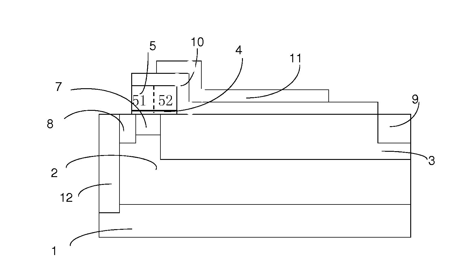
The present invention provides an RF LDMOS device that can be easily manufactured and is capable of mitigating the HCI effect while not increasing the on-resistance. The device has a gate structure containing two sections having different dopant concentrations, which leads to a maximum inhibition of polysilicon depletion and a certain amount of polysilicon depletion upon the application of a backward biasing voltage on the gate structure. These technical effects facilitate the reduction of electric field in the channel region and mitigate the HCI effect in the normal bias state.
Problems solved by technology
However, a high dopant concentration of the N-type drift region 3 may also lead to some consequences detrimental to the reliability of the device, in particular the intensification of the so-called hot carrier injection (HCI) effect.
However, this approach will decrease the on-resistance of the device.
Furthermore, while making a step-shaped gate oxide layer 4 whose thickness is larger in one section proximal to the drain region 9 than in the other section near to the source region 8 can enable an unchanged on-resistance of the device even when the N-type drift region 3 is heavily doped, such a complex structure of the step-shaped gate oxide layer 4 will increase the complexity of the fabrication process.
Method used
Image
Click on the blue label to locate the original text in one second.
Reading with bidirectional positioning of images and text.
Examples
first embodiment
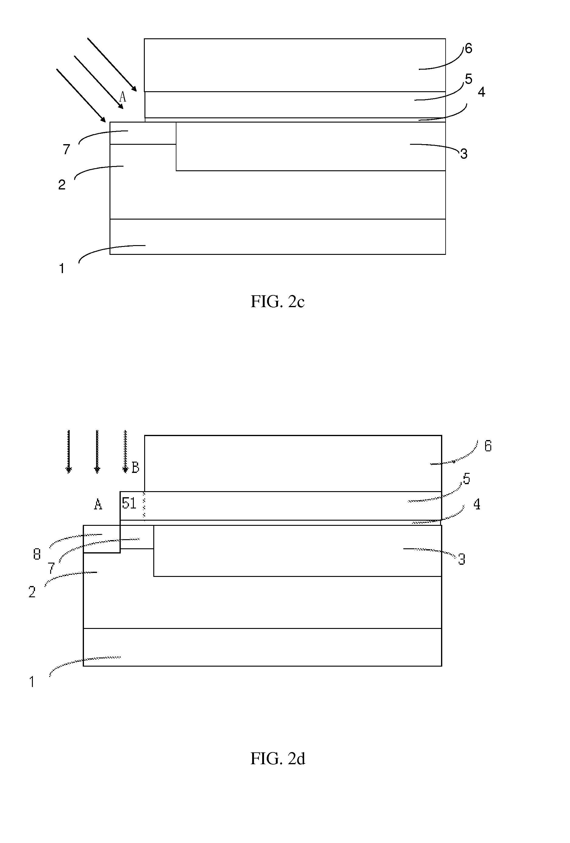
[0031]In a first embodiment, the method includes the nine steps 1 to 9 as described below, which can be better understood when read in conjunction with FIGS. 2a to 2i.
[0032]In step 1, referring to FIG. 2a, a lightly-doped P-type epitaxial layer 2 is first formed over a heavily-doped P-type substrate 1, and thereafter a photolithography process using photoresist as a mask is performed, followed by one or more ion implantations, to form an N-type drift region 3 in the epitaxial layer 2.
[0033]As a variant, in step 1, forming the epitaxial layer 2 may be omitted, and accordingly, the drift region 3 and several other components as described below are formed directly in or on the substrate 1 instead.
[0034]In step 2, referring to FIG. 2b, a thermal oxidation process is employed to grow a siliconoxide layer 4 on a surface of the silicon material layer (including both the drift region 3 and a portion of the epitaxial layer 2), followed by depositing a polysilicon layer 5 over the entire su...
second embodiment
[0047]In a second embodiment, the method includes the following nine steps 1′ to 9′ as described below, which can be better understood by referencing FIGS. 3a to 3i.
[0048]As seen in FIGS. 3a and 3b, steps 1′ and 2′ of this embodiment are the same as the corresponding steps 1 and 2 of the first embodiment.
[0049]In step 3′, referring to FIG. 3c, photolithography and etching processes are performed to shape the silicon oxide layer and polysilicon layer into a gate oxide layer 4 and a polysilicon gate structure 5, respectively. The gate oxide layer 4 has a portion overlying the epitaxial layer 2 and the rest portion overlying the drift region 3.
[0050]In step 4′, referring to FIG. 3d, a photolithography process is performed to form, in a photoresist layer 6, an opening D exposing a portion of the epitaxial layer 2 on one side of the polysilicon gate structure 5 and a first section 51 of the polysilicon gate structure 5 away from the drift region 3, with a second section 52 of the polysi...
PUM
Abstract
A radio frequency (RF) laterally diffused metaloxidesemiconductor (LDMOS) device is disclosed, which includes: a gate structure on a surface of a substrate; and a source region and a drain region beneath the surface of the substrate, the source region and the drain region formed on opposite sides of the gate structure, wherein the gate structure includes a first section proximal to the source region and a second section proximal to the drain region, and wherein the first section of the gate structure has a dopant concentration at least one decimal order higher than a dopant concentration of the second section of the gate structure. A method of forming an RF LDMOS device is also disclosed. With the gate structure including two sections having different dopant concentrations, the present invention is capable of reducing the hot carrier injection effect while possessing a low on-resistance.
Description
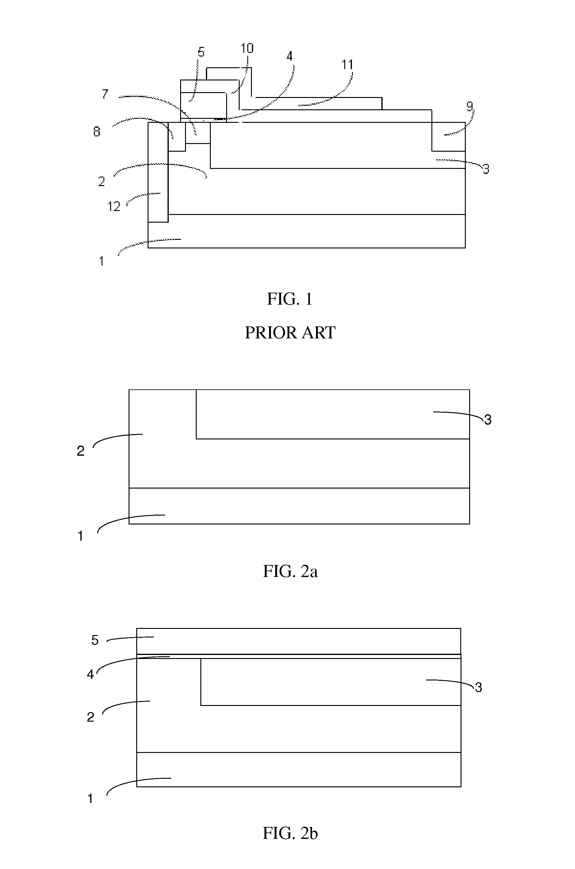
CROSS-REFERENCES TO RELATED APPLICATIONS[0001]This application claims the priority of Chinese patent application number 201210521428.1, filed on Dec. 7, 2012, the entire contents of which are incorporated herein by reference.TECHNICAL FIELD[0002]The present invention relates generally to semiconductor devices, and in particular, to a laterally diffused metaloxidesemiconductor (LDMOS) device usable in radio frequency (RF) applications.BACKGROUND[0003]RF LDMOS devices are commonly used in RF base stations and RF broadcast stations. Manufacturers are always pursuing RF LDMOS devices having a high breakdown voltage, low on-resistance and low parasitic capacitance.[0004]FIG. 1 shows an existing RF LDMOS device, which can be either a P-channel or N-channel one. In the case of an N-channel RF LDMOS device, as illustrated in FIG. 1, the reference number 1 represents a heavily-doped P-type substrate whereon a lightly-doped P-type epitaxial layer 2 is formed. In the lightly-doped P-type epi...
Claims
Application Information
Patent Timeline
Application Date:The date an application was filed.
Publication Date:The date a patent or application was officially published.
First Publication Date:The earliest publication date of a patent with the same application number.
Issue Date:Publication date of the patent grant document.
PCT Entry Date:The Entry date of PCT National Phase.
Estimated Expiry Date:The statutory expiry date of a patent right according to the Patent Law, and it is the longest term of protection that the patent right can achieve without the termination of the patent right due to other reasons(Term extension factor has been taken into account ).
Invalid Date:Actual expiry date is based on effective date or publication date of legal transaction data of invalid patent.

