Heat treatment apparatus for heating substrate by irradiation with flash light

a technology of heat treatment apparatus and substrate, which is applied in the direction of lighting and heating apparatus, drying machines, furnaces, etc., can solve the problems of warping deformation of semiconductor wafers, too deep junction depth and possible impediments, and semiconductor wafers may jump off the susceptor, so as to prevent cracks in the substrate

Inactive Publication Date: 2014-06-19
DAINIPPON SCREEN MTG CO LTD
View PDF6 Cites 27 Cited by
  • Summary
  • Abstract
  • Description
  • Claims
  • Application Information

AI Technical Summary

Benefits of technology

[0019]When the fallen substrate collides with the tapered surface, the substrate can smoothly slide along the tapered surfa

Problems solved by technology

If, at this time, the annealing time is about several seconds or more, the implanted impurities will be diffused deeply by heat, which may result in too deeper a junction depth and a possible impediment to the formation of a favorable device.
Thus, the surface temperature of the semiconductor wafer rapidly increases in a moment and causes abrupt thermal expansion in the wafer surface, resulting in warping deformation of the semiconductor wafer.
At this time, if a gap is formed by the support pins between the back face of semiconductor wafer and the top face

Method used


Image

  • Heat treatment apparatus for heating substrate by irradiation with flash light
  • Heat treatment apparatus for heating substrate by irradiation with flash light
  • Heat treatment apparatus for heating substrate by irradiation with flash light

Examples


Embodiment Construction

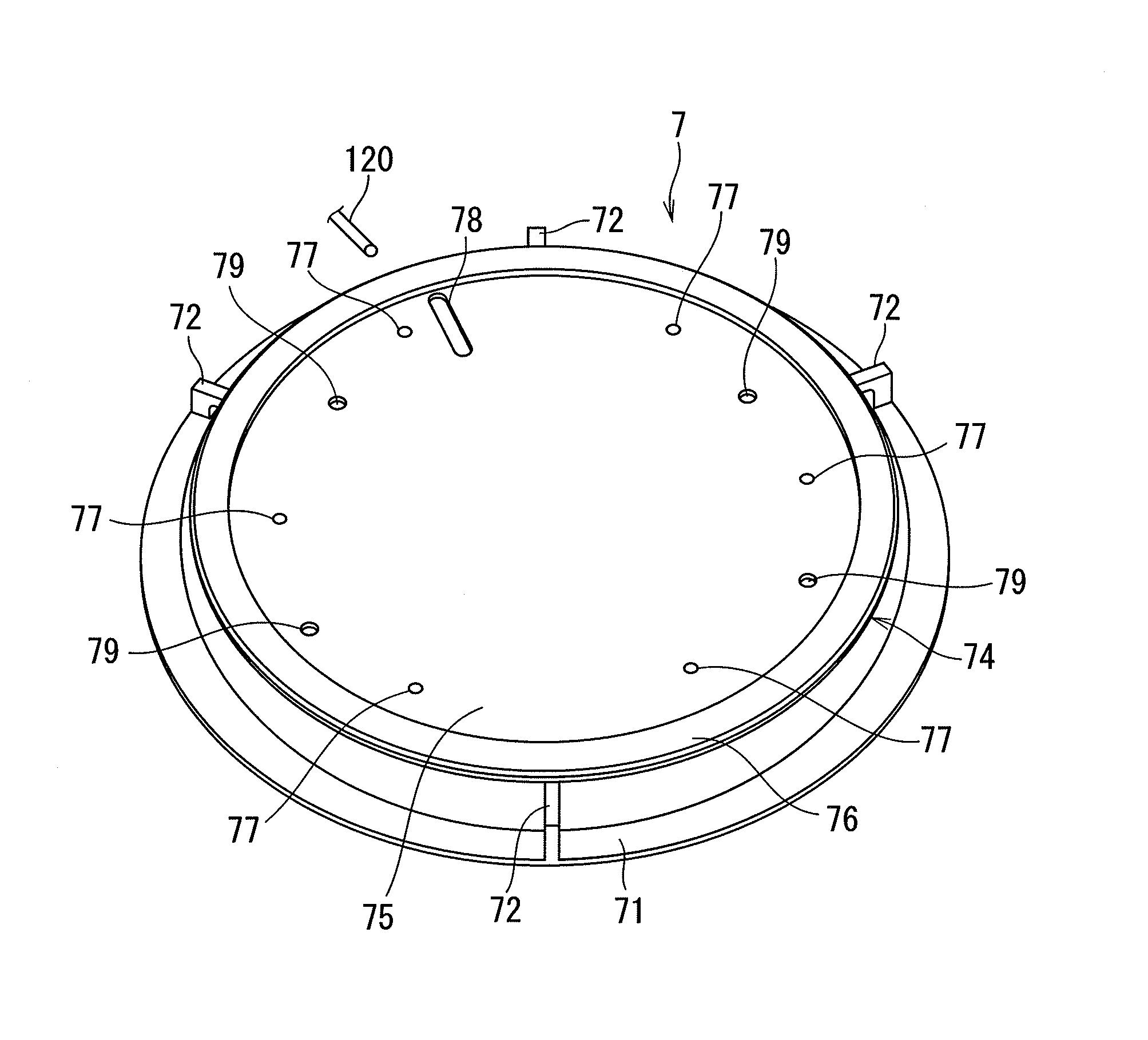
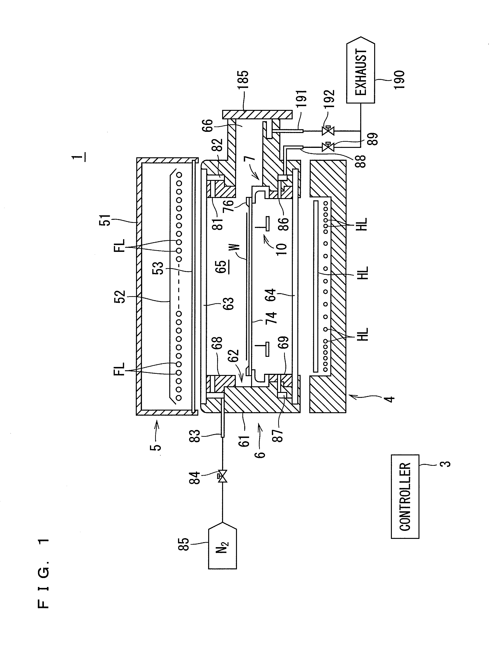
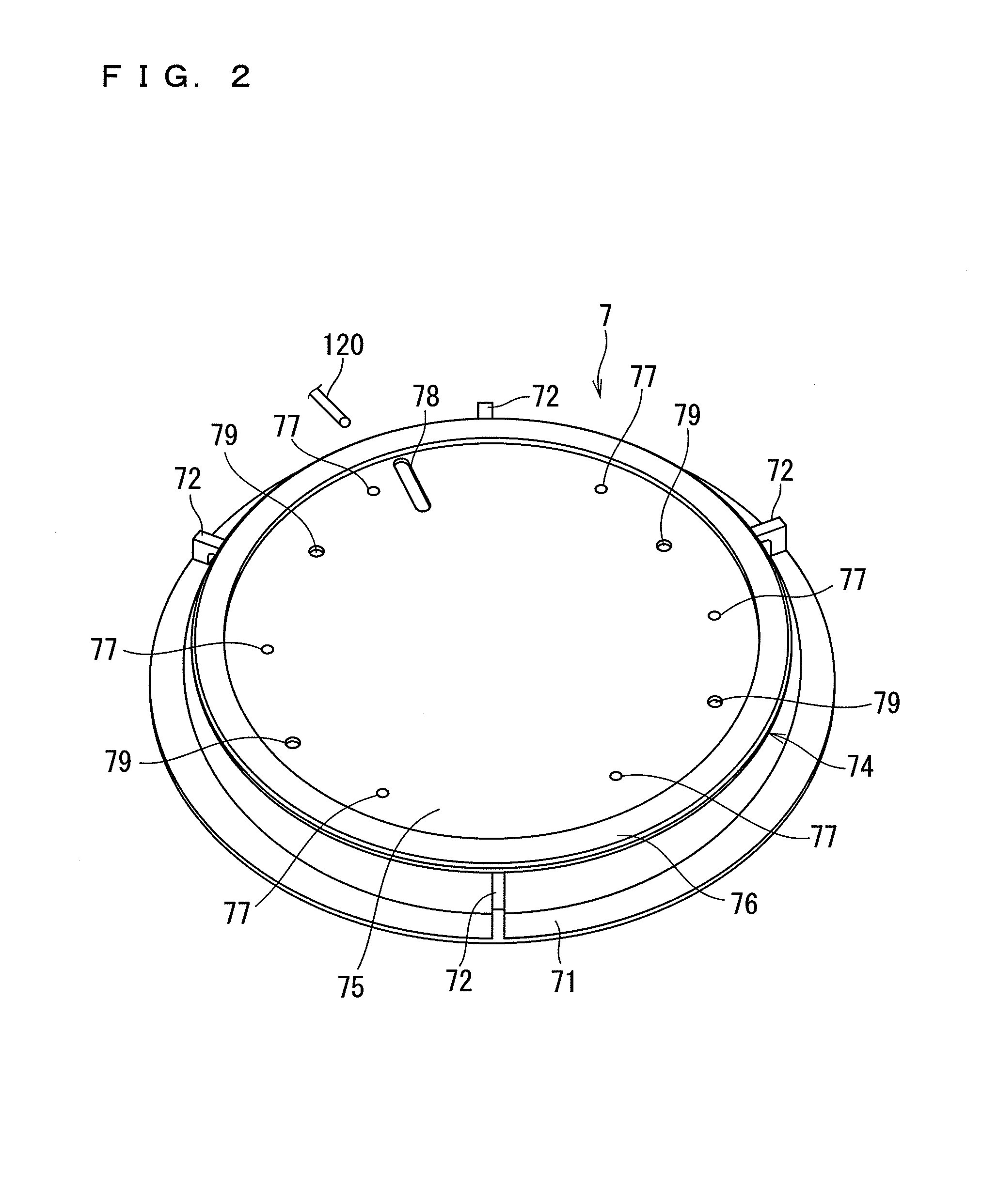
[0034]FIG. 1 is a longitudinal cross-sectional view showing a configuration of a heat treatment apparatus 1 according to the present invention. The heat treatment apparatus 1 of the present embodiment is a flash-lamp annealing apparatus for heating a disc-shaped semiconductor wafer W serving as a substrate by applying flash light to the semiconductor wafer W. Although there is no particular limitation on the size of the semiconductor wafer W to be treated, the semiconductor wafer W may have a diameter of 300 mm or 450 mm, for example. The semiconductor wafer W is implanted with impurities before being transported into the heat treatment apparatus 1, and treatment for activating the implanted impurities is performed through heat treatment by the heat treatment apparatus 1. To facilitate the understanding, the size and number of each part are exaggerated or simplified as necessary in FIG. 1 and subsequent drawings.

[0035]The heat treatment apparatus 1 includes a chamber 6 for accommoda...


PUM


Abstract

A susceptor of a holding part for holding a semiconductor wafer includes a disc-shaped holding plate, an annular shaped guide ring, and a plurality of support pins. The guide ring has an inside diameter greater than the diameter of the semiconductor wafer and is installed on the peripheral portion of the top face of the holding plate. The guide ring has a tapered surface along the inner circumference. The semiconductor wafer before irradiated with flash light is supported by the support pins. The annular shape of the guide ring increases the contact area when the semiconductor wafer that has jumped off the susceptor and fallen when irradiated with flash light collides with the guide ring, thus reducing the impact of the collision and preventing cracks in the substrate.

Description

BACKGROUND OF THE INVENTION[0001]1. Field of the Invention[0002]The present invention relates to a heat treatment apparatus for heating a sheet precision electronic substrate (hereinafter, simply referred to as a “substrate”) such as a disc-shaped semiconductor wafer by applying flash light to the substrate.[0003]2. Description of the Background Art[0004]In the manufacturing process of a semiconductor device, the introduction of impurities is an essential step for forming pn junctions in a semiconductor wafer. Currently, it is common to use ion implantation and subsequent annealing to introduce impurities. Ion implantation is a technique by which impurity elements such as boron (B), arsenic (As), and phosphorus (P) are ionized and caused to collide with a semiconductor wafer at a high acceleration voltage to physically implant impurities. The implanted impurities are activated by annealing treatment. If, at this time, the annealing time is about several seconds or more, the implante...

Claims


Application Information

Patent Timeline
IPC IPC(8): H01L21/687H01L21/67
CPCH01L21/67115H01L21/68735H01L21/6875H01L21/324H05B3/0047
Inventor ABE, MAKOTOYAMADA, TAKAHIROFUSE, KAZUHIKO
Owner DAINIPPON SCREEN MTG CO LTD
Why Eureka
Try Eureka