

Semiconductor device manufacturing method
a technology of semiconductor devices and manufacturing methods, applied in the direction of semiconductor devices, basic electric elements, electrical appliances, etc., can solve the problems of reducing the data holding capacity of nand-flash memory, excessively small actually difficult to do, so as to reduce the amount of electric charge trapped at the ono film for charge trapping, reduce the displacement of channel holes, and reduce the effect of “wiggling”
- Summary
- Abstract
- Description
- Claims
- Application Information
AI Technical Summary
Benefits of technology
Problems solved by technology
Method used
Image

Examples
first embodiment
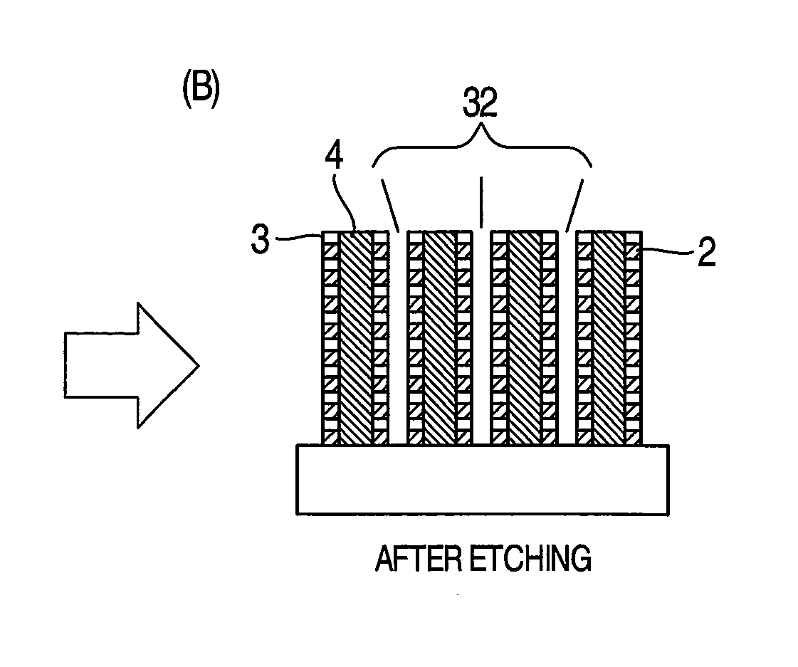
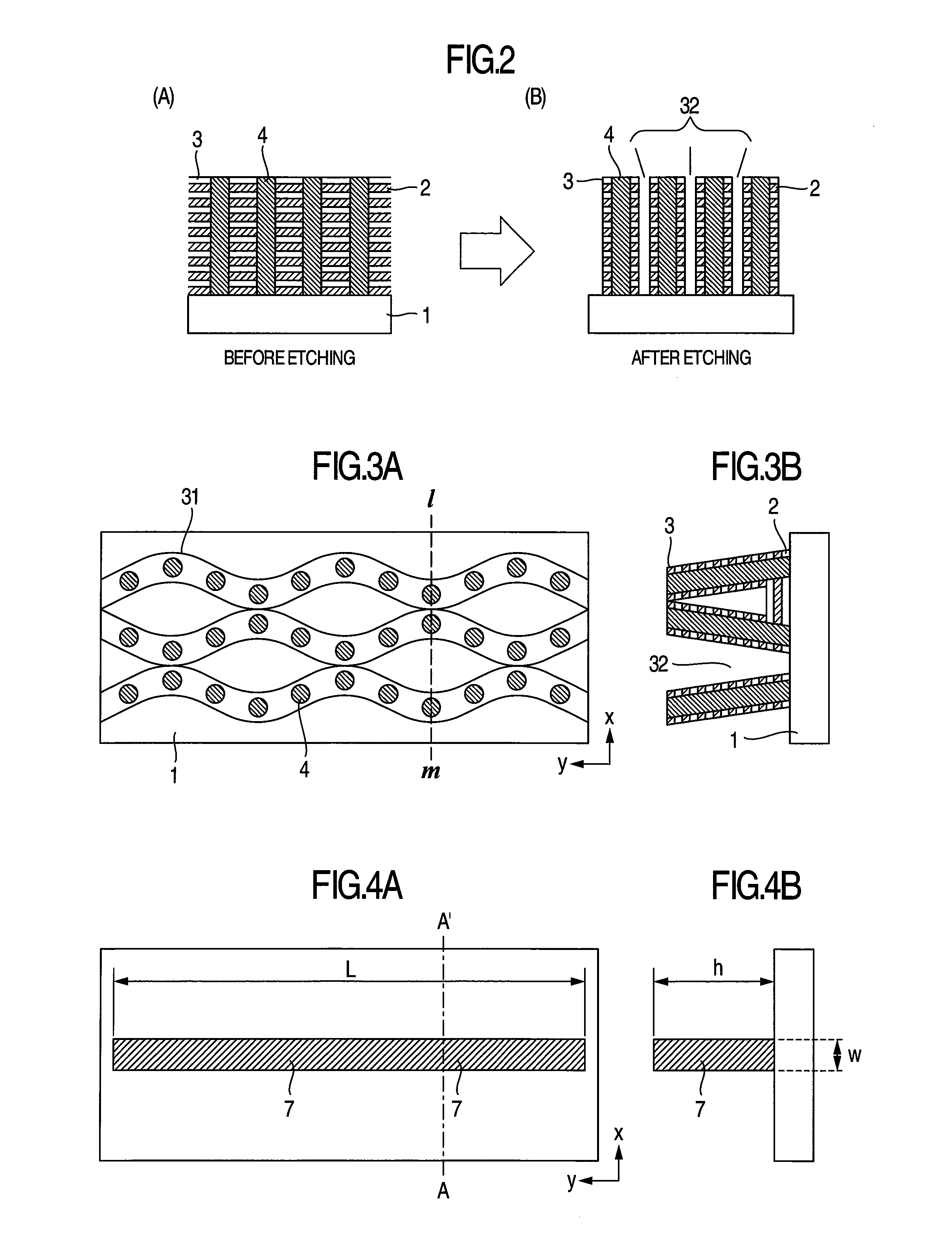
[0048]First, a mechanism that “wiggling” occurs in a semiconductor device, which is provided with a semiconductor element block of a line-and-space form, is described referring to a line pattern formed of a single layer film as an example.
[0049]As described previously, the control gate layer of the 3D-NAND has a SiO2 film deposited and formed on a Si3N4 film by CVD in the initial stage of the manufacturing process. It is known that a material formed by CVD, not limited to 3D-NAND manufacturing processes, has a very small residual stress when the film is formed. It was also found that when the multi-layered film of the control gate layer is fabricated into lines and spaces by etching, a stress is generated in the multi-layered film as the multi-layered film deteriorates in the etching process, and the multi-layered film is deformed by the stress. Therefore, “wiggling” is considered to occur due to two factors of the above-described residual stress and the deterioration of the multi-l...
second embodiment
[0061]With this embodiment an example is described in which “wiggling” due to buckling is suppressed by applying the method described in the first embodiment to the 3D-NAND manufacturing process.
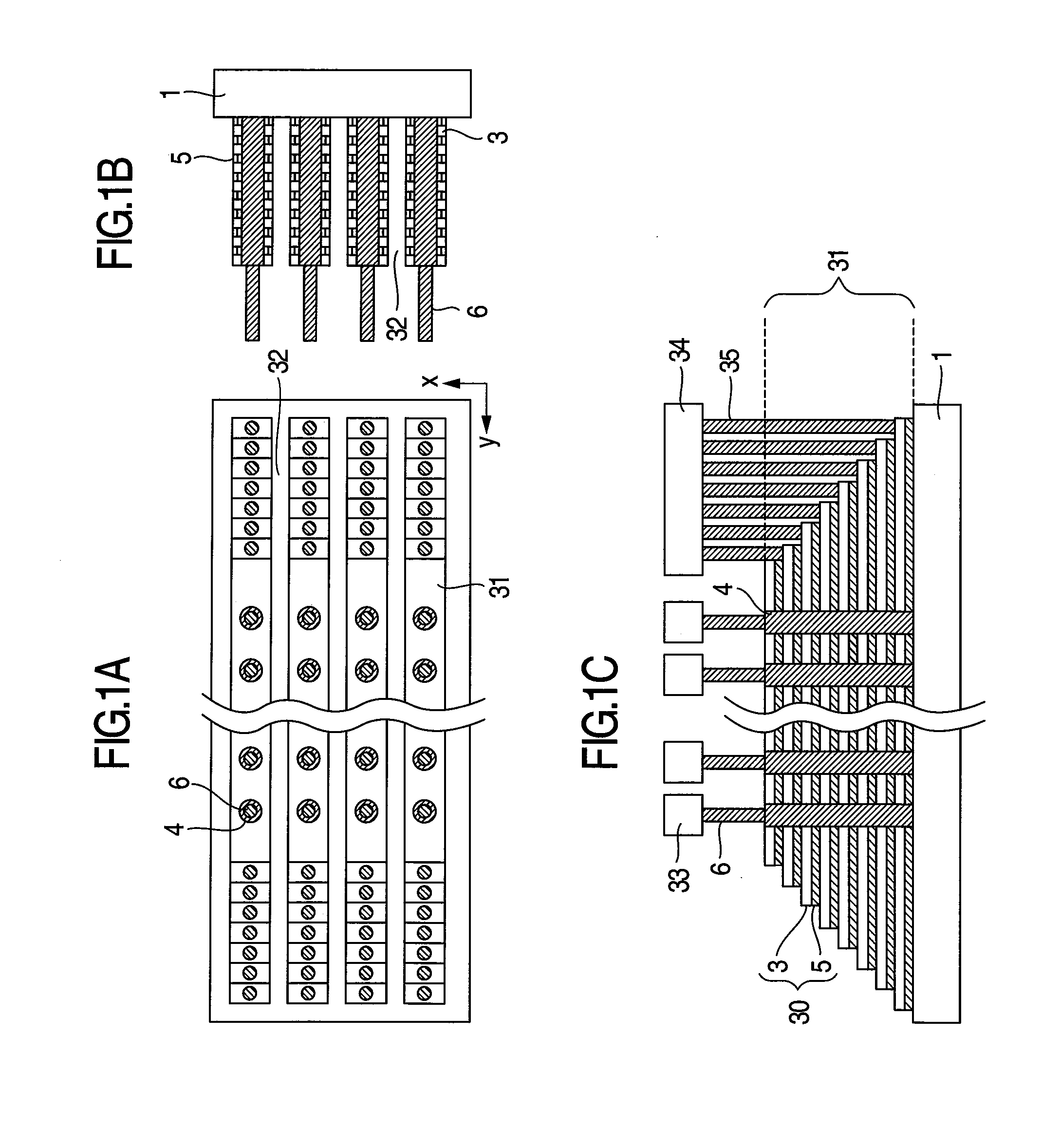
[0062]FIG. 7 shows an appearance view of a die forming a 3D-NAND of this embodiment. The die shown in FIG. 7 has a structure that four sets of a memory cell 70 and a peripheral circuit 71 of the 3D-NAND are integrated. The structure of each memory cell is substantially the same as that of the memory cell shown in FIG. 1, but the aspect ratio of the control gate group 31 is defined to be a value with which buckling does not occur easily.
[0063]Next, the structure of the 3D-NAND having the occurrence of buckling and the structure of the 3D-NAND in which buckling does not occur are described in comparison with each other. As described above, buckling occurs when a multi-layered film of Si3N4 films 2 and SiO2 films 3 is etched to separate and form the line-and-space pattern by forming trenches 32...
third embodiment
[0082]In this embodiment, a waviness amplification phenomenon which is another “wiggling” mechanism and a principle for suppressing waviness amplification are described. A mask formed by lithography has a defect which is called Line-Edge-Roughness (LER) and has a characteristic that the line pattern mask waves by about several nanometers. The phenomenon that large “wiggling” is caused to occur by the waviness is a waviness amplification phenomenon. For example, it is assumed that there is a line pattern 7 waving in right and left sinusoidally with a cycle λ as shown in FIG. 18A. FIG. 18B shows a cross-sectional view taken along the line A-A′ of FIG. 18A, and in this state, it is self-standing without falling. Letting the amplitude of a sine wave representing waviness virtually be a0 / 2, the position coordinate of this pattern is expressed by the following expression.
[MATH.3]x=a02sin(yλ)(3)
[0083]When the material forming the pattern has a residual stress σ, a force F that deforms the ...
PUM
 Abstract
Description
Claims
Application Information