Recipe generation apparatus, inspection support apparatus, inspection system, and recording media

a technology of generating apparatus and recording media, which is applied in the direction of semiconductor/solid-state device testing/measurement, image enhancement, instruments, etc., can solve the problems of layout-dependent defects called systematic defects, defects may arise in the boundary of a memory part and other areas of the design layout, and the ratio of defects that depend on the design layout has been increasing, so as to achieve simple extraction principle and reduce the time required for arithmetic processing. , the effect of increasing the speed

Inactive Publication Date: 2014-06-26
HITACHI HIGH-TECH CORP
View PDF6 Cites 13 Cited by
  • Summary
  • Abstract
  • Description
  • Claims
  • Application Information

AI Technical Summary

Benefits of technology

[0023]According to the present invention, it becomes possible to extract the object area of desired inspection, observation, or measurement directly from the design layout data and at higher speed than before. A time required for arithmetic processing is shorter than the conventional method because an extraction principle is simple, and therefore it becomes possible to perform recipe generation in a shorter time than before and simply.
[0024]Moreover, according to the present invention, since the tool that associates the analysis result of the hierarchical structure of the design layout data and the layout pattern is provided, it becomes possible to simply set the object area of the desired inspection, observation, or measurement.

Problems solved by technology

However, as microfabrication of the semiconductor device proceeds into a finer stage in recent years, a ratio of defects that depend on the design layout has been increasing.
The layout-dependent defects are called systematic defects.
Moreover, a defect may arise in a boundary of a memory part and other areas in the design layout.
A pattern density becomes uneven easily in the above-mentioned boundary part, such unevenness causes abnormalities to occur in manufacturing processes of the semiconductor device such as lithography, CMP, and etching, and consequently a defect is generated.
However, with a progress of pattern microfabrication in recent years, cases where a minute defect is overlooked with the optical defect inspection apparatus because of a limit of its resolution have increased.
On the other hand, in the electron beam system, although its resolution satisfies the requirement, an inspectable area per unit time is limited, and there was a problem that neither an entire wafer surface nor an entire chip surface could be inspected within a practical time.
What becomes a problem here is how to manage to perform specification of the place to be inspected by the electron beam and setting of inspection conditions at that time in a short time and simply.

Method used


Image

  • Recipe generation apparatus, inspection support apparatus, inspection system, and recording media
  • Recipe generation apparatus, inspection support apparatus, inspection system, and recording media
  • Recipe generation apparatus, inspection support apparatus, inspection system, and recording media

Examples


first embodiment

[0037]In this embodiment, an embodiment of a recipe generation apparatus for executing processing of extracting a peripheral area of the memory mat (hereinafter, referred to a mat end) in patterns formed on a semiconductor wafer as an inspection area will be described. Hereinafter, this embodiment will be explained referring to drawings.

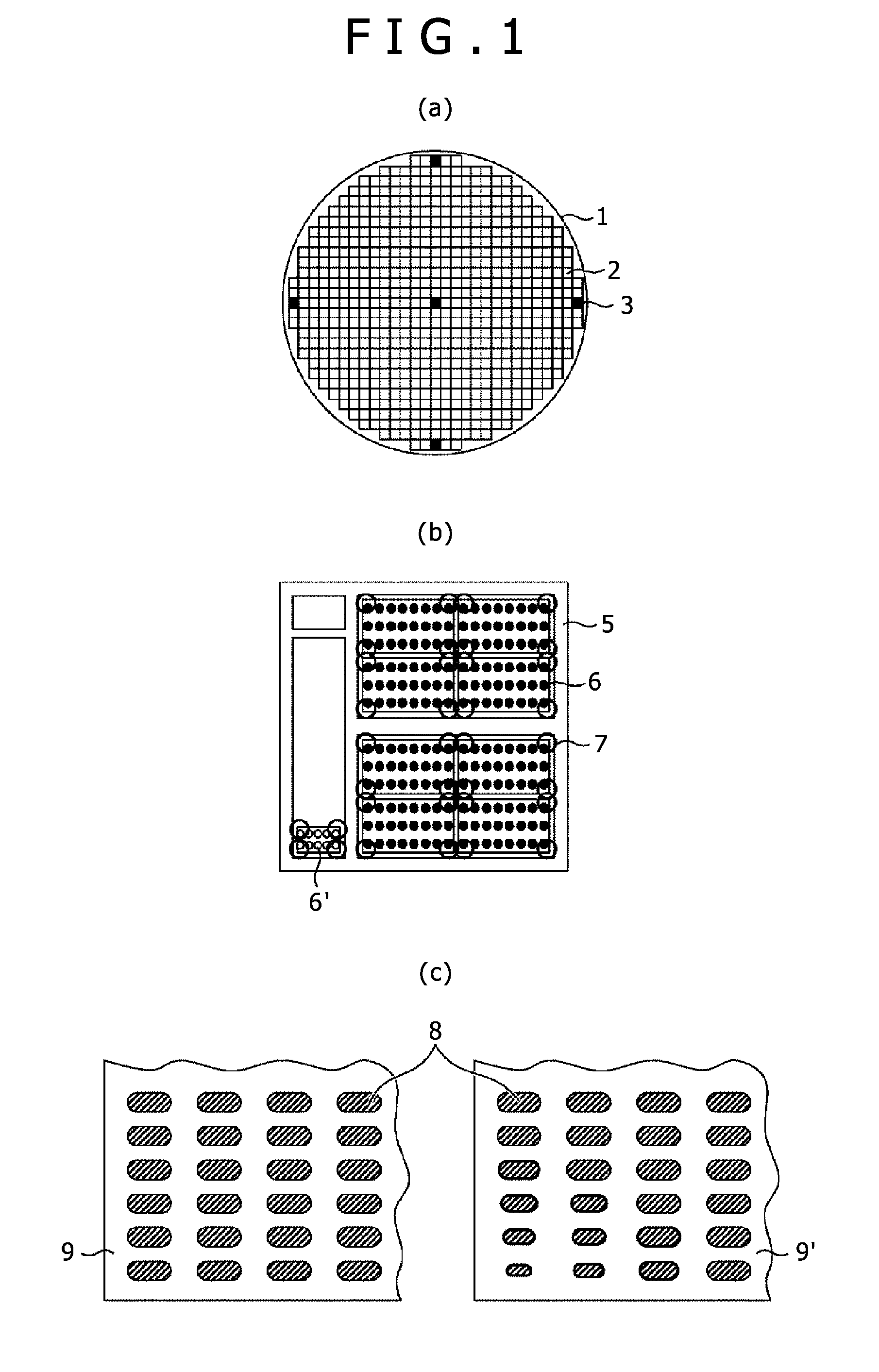
[0038]First, an outline of mat end inspection will be explained using FIG. 1. FIG. 1 (a) schematically shows an appearance of chips 2 are arranged on a wafer 1 that is an inspection object. In the inspection, there is a case where all the chips on the wafer 1 become the inspection objects, and there is also a case where an extraction inspection that specifies an inspection chip 3 is performed.

[0039]FIG. 1 (b) shows a design layout 5 of the chip 2. On the design, the design layout of the inspection chip 3 is the same as that of the chip 2. FIG. 1 (b) shows a chip of a structure where eight memory mats A6 and one memory mat B6′ are mounted on a single ...

second embodiment

[0109]The first embodiment explained the inspection area setting method of specifying the cell corresponding to the target pattern by specifying the lowermost cell or the uppermost cell about a specific tree of the cell hierarchical structure, and tracing the specific tree from the lowermost cell side or the uppermost cell side.

[0110]Such an inspection area setting method is extremely effective when repeatability of the pattern in the chip is high, for example, when the memory mat occupies almost the entire chip layout. However, in areas where the repeatability is low such as a circumference circuit and a logic circuit, a probability that a pattern corresponding to the uppermost cell or the lowermost cell is an already known pattern is low and it is difficult to specify a tree that certainly contains the target pattern.

[0111]Therefore, in this embodiment, a setting technique of the inspection area whereby an arbitrary pattern on the layout pattern or an arbitrary cell on the cell hi...

third embodiment

[0121]This embodiment explains an apparatus of a configuration such that the analysis function of the design layout data explained in the first and second embodiments is set to be independent from the recipe generation apparatus as a different unit (an inspection support apparatus).

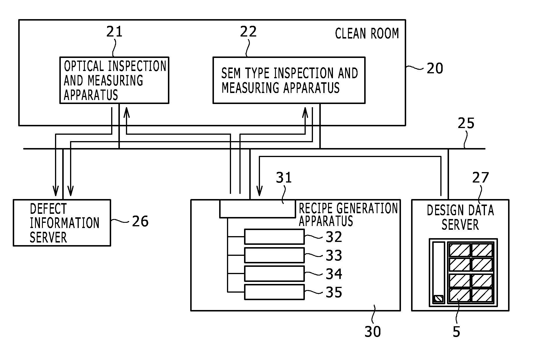
[0122]FIG. 11 shows an arrangement of the inspection support apparatus of this embodiment and various apparatuses connected to the inspection support apparatus. A configuration of this embodiment is the same as the configuration shown in FIG. 3 in respects that various apparatuses such as the defect information server 26 and the design data server 27 are connected with the optical inspection and measuring apparatus 21 or the SEM type inspection and measuring apparatus 22 installed in the clean room 20 through the communication network 25. However, the case of this embodiment differs from the arrangement of FIG. 3 in the following respects: the network interface 31, the storage device 32, the processor 33,...


PUM


Abstract

A desired area is extracted by directly analyzing information recorded in a design layout, an inspection recipe is generated by using this extraction method, and an efficient inspection is realized. The invention makes it easy to extract an area of a desired circuit module such as a memory mat by analyzing hierarchy information of design layout data, calculating reference frequency of each one cell in the design layout data that is its internal data, sorting the cells in order of increasing reference frequency, searching the object, and tracing its upper cell.

Description

TECHNICAL FIELD[0001]The present invention relates to a method for, at the time of inspection, measurement, or reviewing a defect of a sample on which a pattern is formed, setting an inspection area, a measurement area, or a reviewing area, an apparatus used for setting the area, or an inspection apparatus or measurement apparatus having a function of executing the setting method of the above-mentioned inspection area.[0002]Moreover, the present invention relates to a recipe generation apparatus for generating an inspection recipe, measurement recipe, or defective reviewing recipe that includes the above-mentioned area setting process in its generation process, or a program used by the recipe generation apparatus, or a recording medium in which the program is stored.BACKGROUND ART[0003]Conventionally, a main cause of yield loss in a semiconductor wafer manufacturing was particles generated at random on a semiconductor wafer, and it was able to maintain the yield by reducing these pa...

Claims


Application Information

Patent Timeline
Patent Type & Authority Applications(United States)
IPC IPC(8): G06T7/00G06F17/50
CPCG06T7/0006G06T2207/10061G06T2207/30148H01L22/12G06F30/398
Inventor NAKAGAKI, RYOHAMAMURA, YUICHIENOMOTO, YUJITANDAI, YUTAKASAKAI, TSUNEHIROHASUMI, KAZUHISA
Owner HITACHI HIGH-TECH CORP
Why Eureka
Try Eureka