Submicro-facet light-emitting device and method for fabricating the same

a submicro-facet and light-emitting technology, which is applied in the direction of semiconductor/solid-state device manufacturing, semiconductor devices, electrical devices, etc., can solve the problems of reducing light extraction efficiency, limited single-chip leds in the prior art in delivering a great deal of lumens, and reducing the efficiency of light extraction, so as to enhance the total current-sustaining capacity and light extraction, a large active-region volume, and a large amount of white light lumens

Inactive Publication Date: 2014-07-10
ZHEJIANG INVENLUX TECH
View PDF3 Cites 10 Cited by
  • Summary
  • Abstract
  • Description
  • Claims
  • Application Information

AI Technical Summary

Benefits of technology

[0006]Disclosed herewith is a light emitting device having a wavy active-region for enlarged active-region volume without increasing the total lateral area of the active-region (while satisfying the requi

Problems solved by technology

A single chip LED in the prior art is limited in delivering a great deal of lumens for several inherent shortcomings.
Firstly, the prior art LEDs are limited in chip size, because light extraction efficiency decreases as chip size increases.
Secondly, the prior art white LEDs suffer from a fact called efficiency droop, characterized in efficiency setback with increasing current density.
The efficiency droop has its physical

Method used


Image

  • Submicro-facet light-emitting device and method for fabricating the same
  • Submicro-facet light-emitting device and method for fabricating the same
  • Submicro-facet light-emitting device and method for fabricating the same

Examples


Embodiment Construction

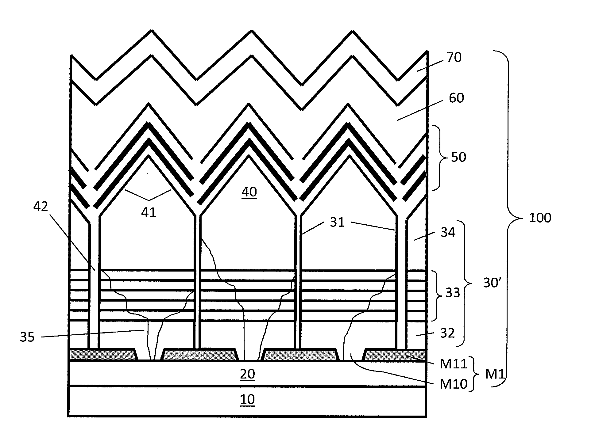
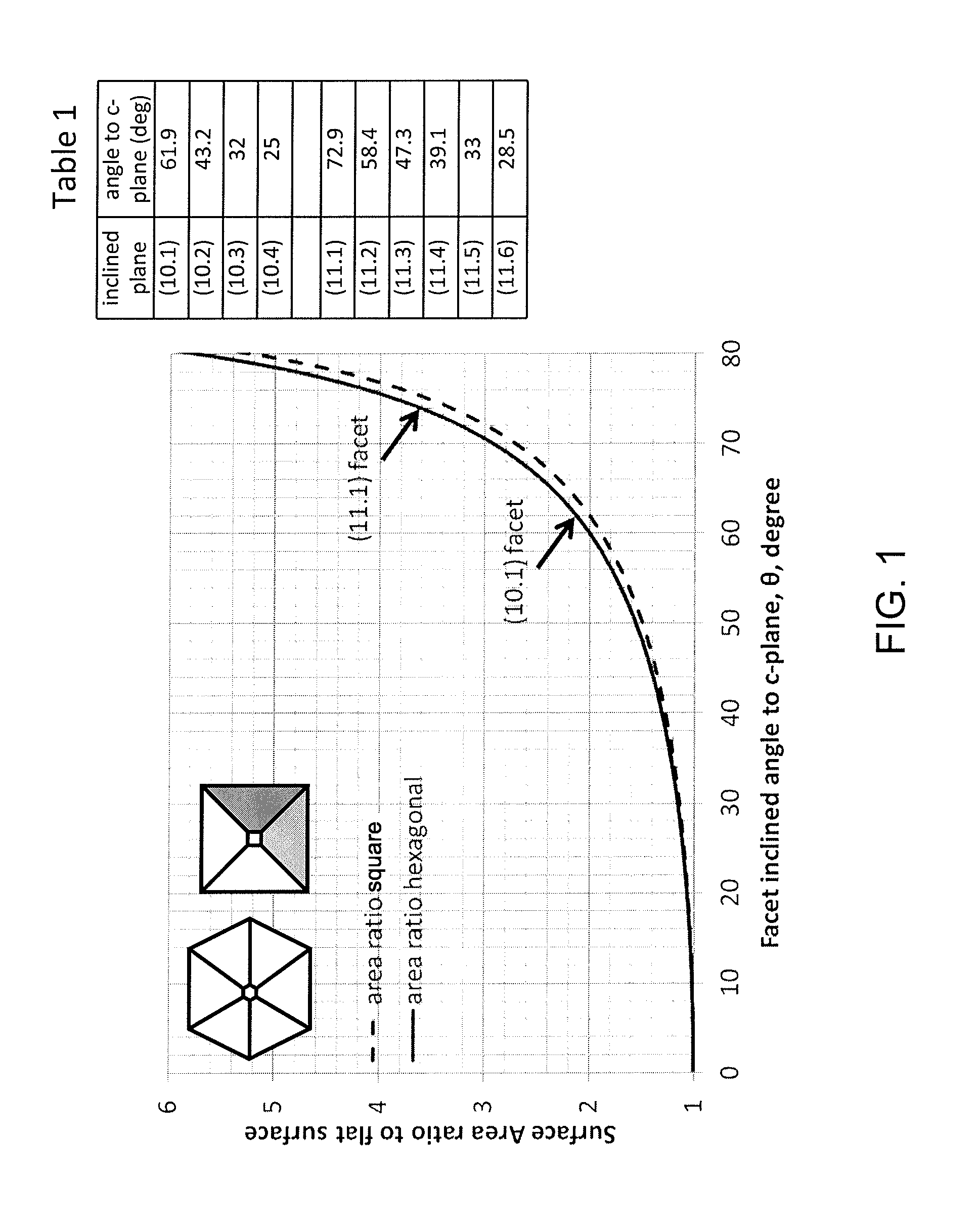
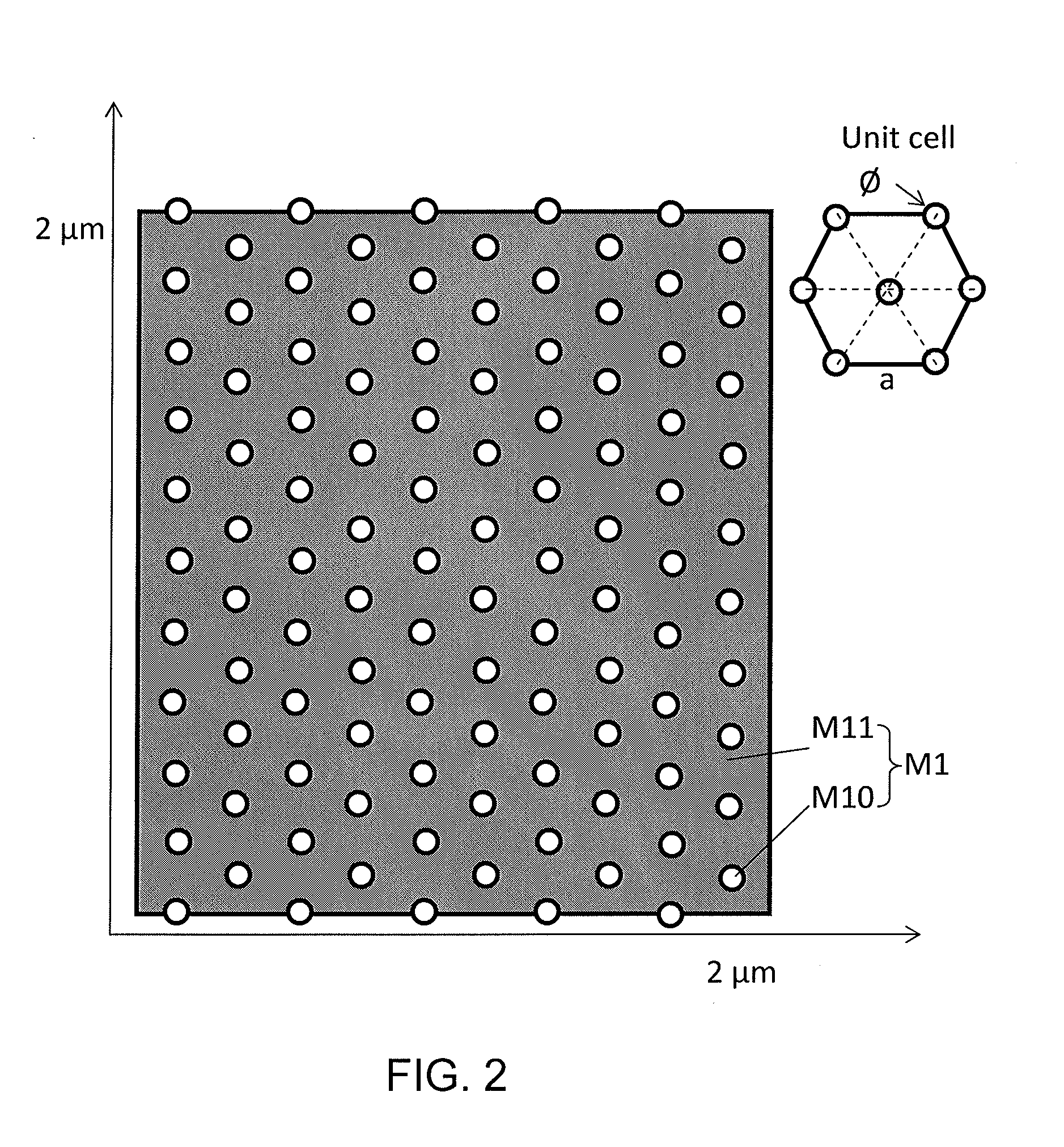
[0048]Disclosed herewith is a light emitting device having submicro-facets for enlarged active-region and enhanced light extraction. In some embodiments, the light-emitting device according to the present invention includes high-density micro or submicro pillars on which an active region is formed. This is to say that these pillars' cross-sectional dimension is in the micron or submicron range, for example, from 500 nm to 1200 nm. The pillars' height, or length, can also be in the submicron to micron range, for example, from 600 nm to 2000 nm. The density of the pillars can be in the range of 5×108 cm−2 to 5×109 cm−2. These pillars have tapering tops formed by crystal facets. In some embodiments, these are c-oriented gallium nitride (GaN) pillars, and the facets are (10.1) or (11.1) facets. The pillars are preferred to be arranged in a close-packed hexagonal pattern (lattice) or square pattern, and the separation between pillars is preferred to be within 100 nm, for example, from 0 ...


PUM


Abstract

A light emitting device comprises an n-type layer, a p-type layer, and an active region sandwiched between the n-type layer and the p-type layer, wherein the active-region has a wavy structure with nano or micro fluctuations in its thickness direction. The n-type layer comprises crystal facets on its upper surface, and the active-region is conformally formed on the upper surface of the n-type layer and substantially follows the shape of the crystal facets so as to form the wavy structure. A method for fabricating the same is also provided.

Description

FIELD OF THE INVENTION[0001]The present invention relates in general to a light-emitting device, such as light emitting diode (LED), more particularly to a light-emitting device having submicron facets, such as III-nitride light-emitting device, and a method for fabricating the same.DESCRIPTION OF THE RELATED ART[0002]III-nitride based light-emitting devices such as light-emitting diodes (LEDs) are widely acknowledged as the next generation light sources and are currently emerging as strong replacement of incandescent and fluorescent lamps in general lighting. For example, the field of interest uses Cerium-doped yttrium aluminum garnet (YAG:Ce) phosphor to convert InGaN multiple-quantum-well (MQW) LED's blue emission into white light, yielding commercial white light LEDs with luminous efficacies in the range of 80-130 lm / W. The R&D White LED luminous efficacy record reported so far has reached 183 lm / W (Y. Narukawa et al, J. Phys. D: Appl. Phys. 43, 354002 (2010).).[0003]For white L...

Claims


Application Information

Patent Timeline
IPC IPC(8): H01L33/04H01L33/00
CPCH01L33/0075H01L33/04H01L33/24H01L33/007
Inventor ZHANG, JIANPING
Owner ZHEJIANG INVENLUX TECH
Why Eureka
Try Eureka