Liquid crystal display device and driving method thereof

a technology of liquid crystal display and driving method, which is applied in the direction of instruments, static indicating devices, etc., can solve the problems of reducing display quality, and the above method cannot be adopted concerning the discharge of charge, and achieve the effect of suppressing the effect of pixel electrode potential due to the influence of lead-in voltag

Active Publication Date: 2014-07-10
SHARP KK
View PDF2 Cites 15 Cited by
  • Summary
  • Abstract
  • Description
  • Claims
  • Application Information

AI Technical Summary

Benefits of technology

[0101]According to a first aspect of the present invention, in the liquid crystal display device that includes the IGZO-GDM, when supply of the power supply voltage PW is cut off, a charge in the pixel formation portion is first discharged, and thereafter, a charge on the scanning signal line, and charges on the first-node and the second-node in the bistable circuit which configures the shift register are discharged. Accordingly, a residual charge in the panel is quickly removed when the power supply is turned off, and occurrence of display failure and operation failure due to existence of a residual charge in the panel is suppressed.
[0102]According to a second aspect of the present invention, in the scanning signal line discharge process, the output control switching element becomes in the ON state with the clock signal being at the ground potential. As for the output control switching element, the clock signal is applied to the second electrode and the third electrode is connected to the output-node. Therefore, a charge on the scanning signal line is discharged. Further, in the second-node discharge process, the first second-node control switching element becomes in the ON state with the reference potential being at the ground potential. As for the first second-node control switching element, the second electrode is connected to the second-node and the reference potential is applied to the third electrode. Therefore, the a charge of the second-node is discharged. Further, in the first-node discharge process, the second first-node control switching element becomes in the ON state with the reference potential being at the ground potential. As for the second first-node control switching element, the second electrode is connected to the first-node and the reference potential is applied to the third electrode. Therefore, a charge of the first-node is discharged. In the manner as described above, when the power supply is turned off, a charge of each node in the panel is sequentially quickly remove

Problems solved by technology

When the power supply of the device is turned on in a state that a residual charge is accumulated in the pixel formation portion, reduction of a display quality, such as occurrence of flic

Method used


Image

  • Liquid crystal display device and driving method thereof
  • Liquid crystal display device and driving method thereof
  • Liquid crystal display device and driving method thereof

Examples


first embodiment

1. First Embodiment

1. 1 Overall Configuration and Operation

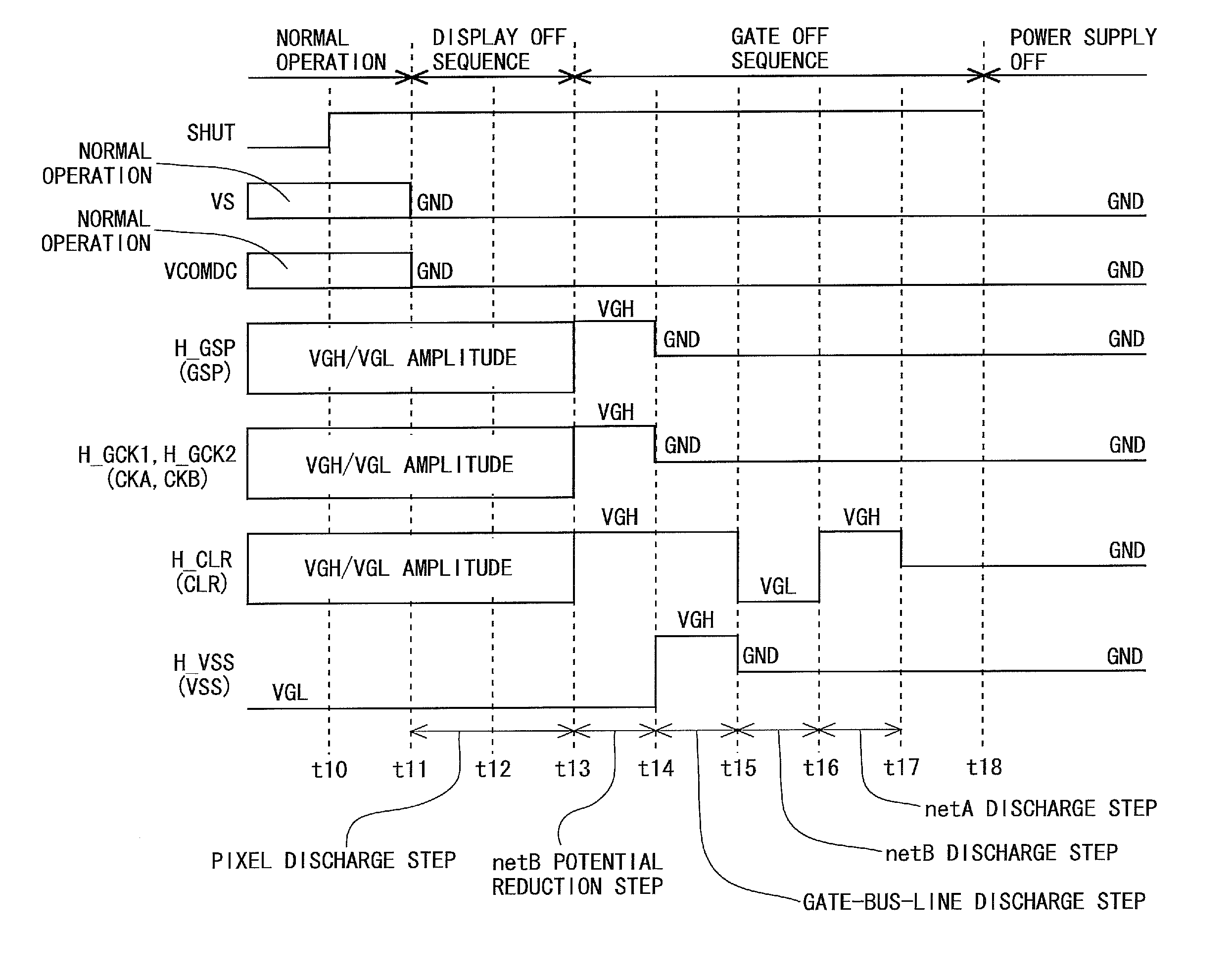
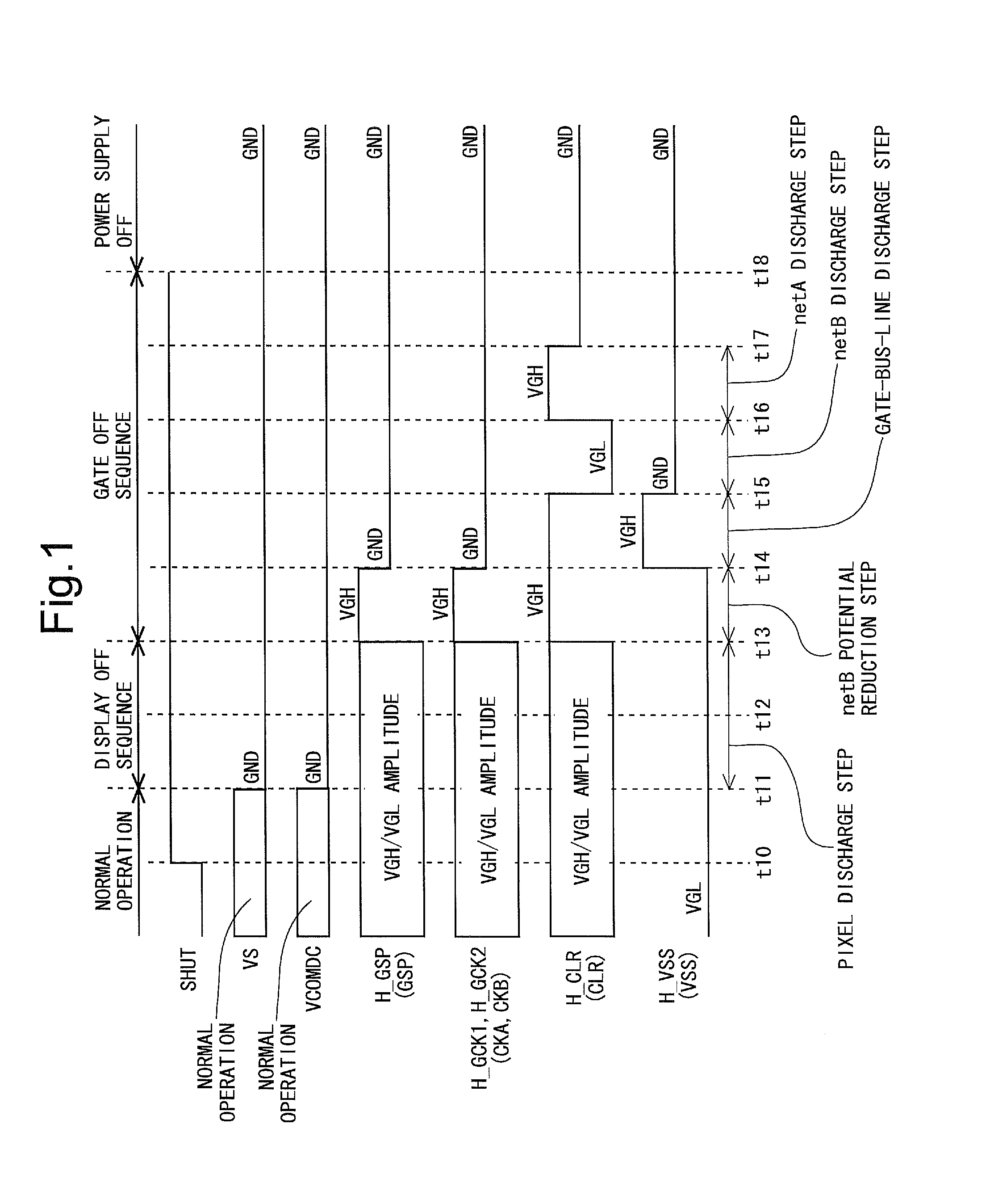
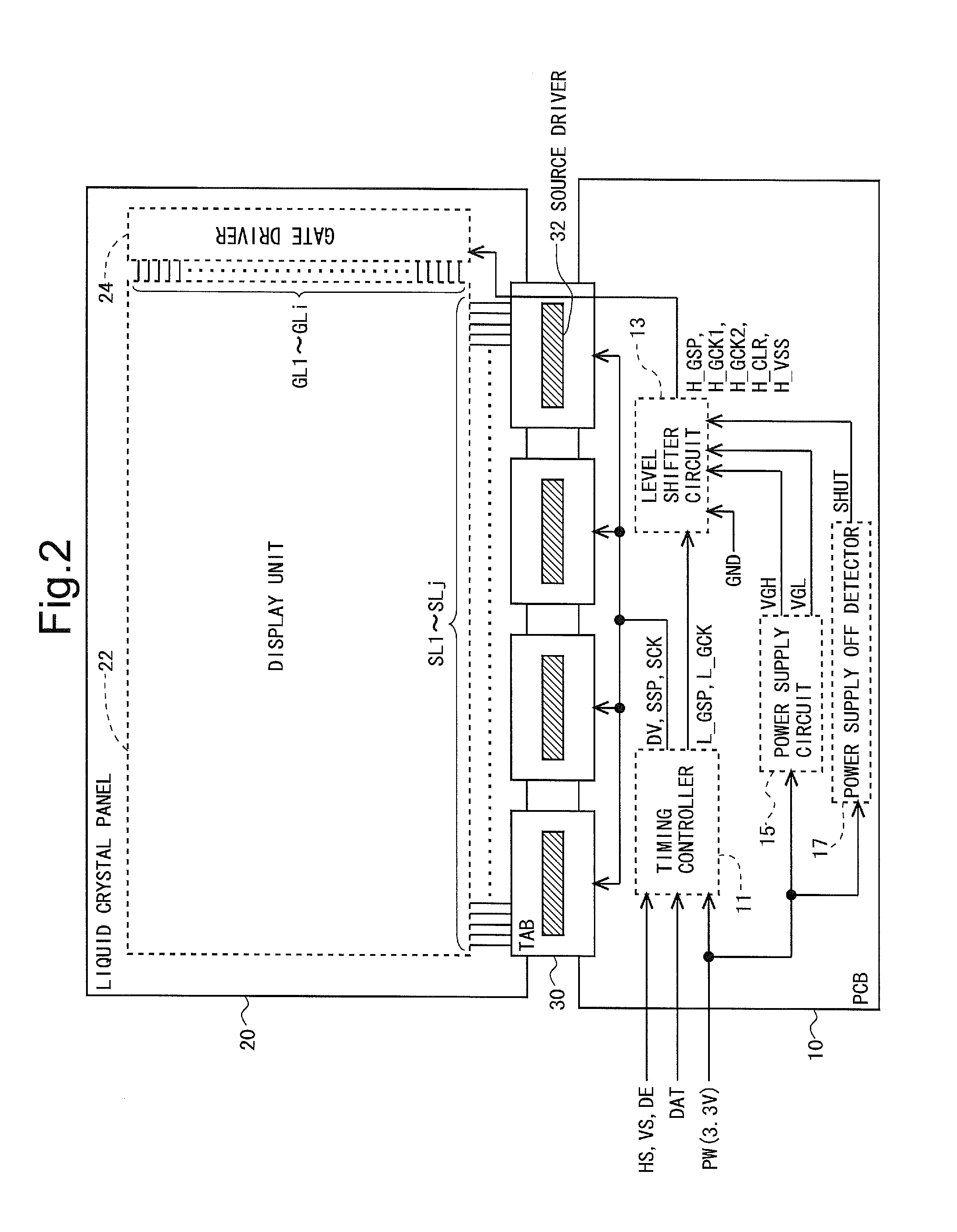
[0139]FIG. 2 is a block diagram showing an overall configuration of an active-matrix type liquid crystal display device according to a first embodiment of the present invention. As shown in FIG. 2, the liquid crystal display device is configured by a liquid crystal panel (display panel) 20, a PCB (printed circuit board) 10, and a TAB (Tape Automated Bonding) 30 connected to the liquid crystal panel 20 and the PCB 10. It should be noted that the liquid crystal panel 20 is an IGZO-TFT liquid crystal panel. The TAB 30 is in a mounting form adopted mainly in a medium-type to large-type liquid crystal panel. In a small-type to medium-type liquid crystal panel, a COG mounting may be adopted as a mounting form of a source driver. Further, recently, a system driver configuration in which a source driver 32, a timing controller 11, a power supply circuit 15, a power supply off detector 17, and a level shifter circuit 13 are set in on...

second embodiment

2. Second Embodiment

[0185]A second embodiment of the present invention is described. It should be noted that only points different from those in the first embodiment are described in detail, and the description of points similar to those in the first embodiment is simplified.

[0186]

[0187]FIG. 15 is a block diagram showing an overall configuration of an active-matrix type liquid crystal display device according to the second embodiment of the present invention. The liquid crystal panel 20 and the TAB have configurations similar to those in the first embodiment. Concerning the PCB 10, although only one power supply off detector 17 is provided in the first embodiment, two power supply off detectors (a first power supply off detector 17a and a second power supply off detector 17b) are provided in the present embodiment. The first power supply off detector 17a sets a power supply state signal SHUT1 to the high level, when a voltage supplied from the power supply voltage PW becomes 2.4 V o...


PUM


Abstract

The invention provides a liquid crystal display device that includes an IGZO-GDM which can quickly remove a residual charge in a panel when the power supply is turned off, and a driving method of the liquid crystal display device. Each bistable circuit that configures a shift register includes a thin film transistor TI for increasing a potential of an output terminal based on a first clock, a region netA connected to a gate terminal of the thin film transistor TI, a thin film transistor TC for lowering a potential of the region netA, and a region netB connected to a gate terminal of the thin film transistor TC. In such a configuration, a power supply off sequence includes a display off sequence and a gate off sequence. The gate off sequence includes at least a gate-bus-line discharge step (t14 to t15), a netB discharge step (t15 to t16), and a netA discharge step (t16 to t17).

Description

TECHNICAL FIELD[0001]The present invention relates to a liquid crystal display device which includes a monolithic gate driver having a thin film transistor using an oxide semiconductor (IGZO) as a semiconductor layer, and a driving method of the liquid crystal display device.BACKGROUND ART[0002]In general, an active-matrix type liquid crystal display device includes a liquid crystal panel formed of two substrates that sandwich a liquid crystal layer in between. On one of the two substrates, there are arranged in a lattice shape a plurality of gate bus lines (scanning signal lines) and a plurality of source bus lines (video signal lines). Further, a plurality of pixel formation portions arranged in a matrix shape are provided respectively corresponding to intersections between the plurality of gate bus lines and the plurality of source bus lines. Each pixel formation portion includes a thin film transistor (TFT) as a switching element having a gate terminal connected to a gate bus li...

Claims


Application Information

Patent Timeline
IPC IPC(8): G09G3/36
CPCG09G3/3611G09G3/3677G09G2330/027
Inventor MORII, HIDEKIIWAMOTO, AKIHISAHORIUCHI, SATOSHIMIZUNAGA, TAKAYUKINAKAMINAMI, KAZUYA
Owner SHARP KK
Why Eureka
Try Eureka