Transistor with longitudinal strain in channel induced by buried stressor relaxed by implantation

a transistor and longitudinal strain technology, applied in the direction of semiconductor devices, basic electric elements, electrical equipment, etc., can solve problems such as reducing channel mobility, and achieve the effect of reducing stress

Active Publication Date: 2014-07-17
ACORN TECH INC
View PDF6 Cites 7 Cited by
  • Summary
  • Abstract
  • Description
  • Claims
  • Application Information

AI Technical Summary

Benefits of technology

[0012]Another aspect of the present invention provides a method of manufacturing a semiconductor device comprising providing a substrate having a semiconductor surface layer. The substrate has a stressor layer positioned at a depth within the substrate and positioned adjacent the semiconductor surface layer and the stressor layer is provided in a stressed state in comparison to the semiconductor surface layer. Trenches are formed to define a region on the substrate having trenches on at least two sides of the region, with two of the trenches defining the region separated by a first lateral extent. A plurality of gate structures are formed above the semiconductor surface layer in the region, with the gate structures extending between the trenches separated by the first lateral extent. First portions of the stressor layer under the gate structures are relaxed so as to strain first portions of the semiconductor surface layer under the gate structures, the relaxing accomplished by implanting ions through second and third portions of the semiconductor surface layer to reduce stress in at least the second and third portions of the stressor layer. Respective source and drain regions are formed in at least a part of the second and third portions of the semiconductor surface layer.

Problems solved by technology

Threading dislocations represent extended defects and give rise to multiple undesirable consequences in MOSFETs including source / drain junction leakage, reduction of channel mobility, variability of threshold voltage and enhanced diffusion paths leading to potential drain-to-source shorting in short-channel MOSFETs.

Method used


Image

  • Transistor with longitudinal strain in channel induced by buried stressor relaxed by implantation
  • Transistor with longitudinal strain in channel induced by buried stressor relaxed by implantation
  • Transistor with longitudinal strain in channel induced by buried stressor relaxed by implantation

Examples


Embodiment Construction

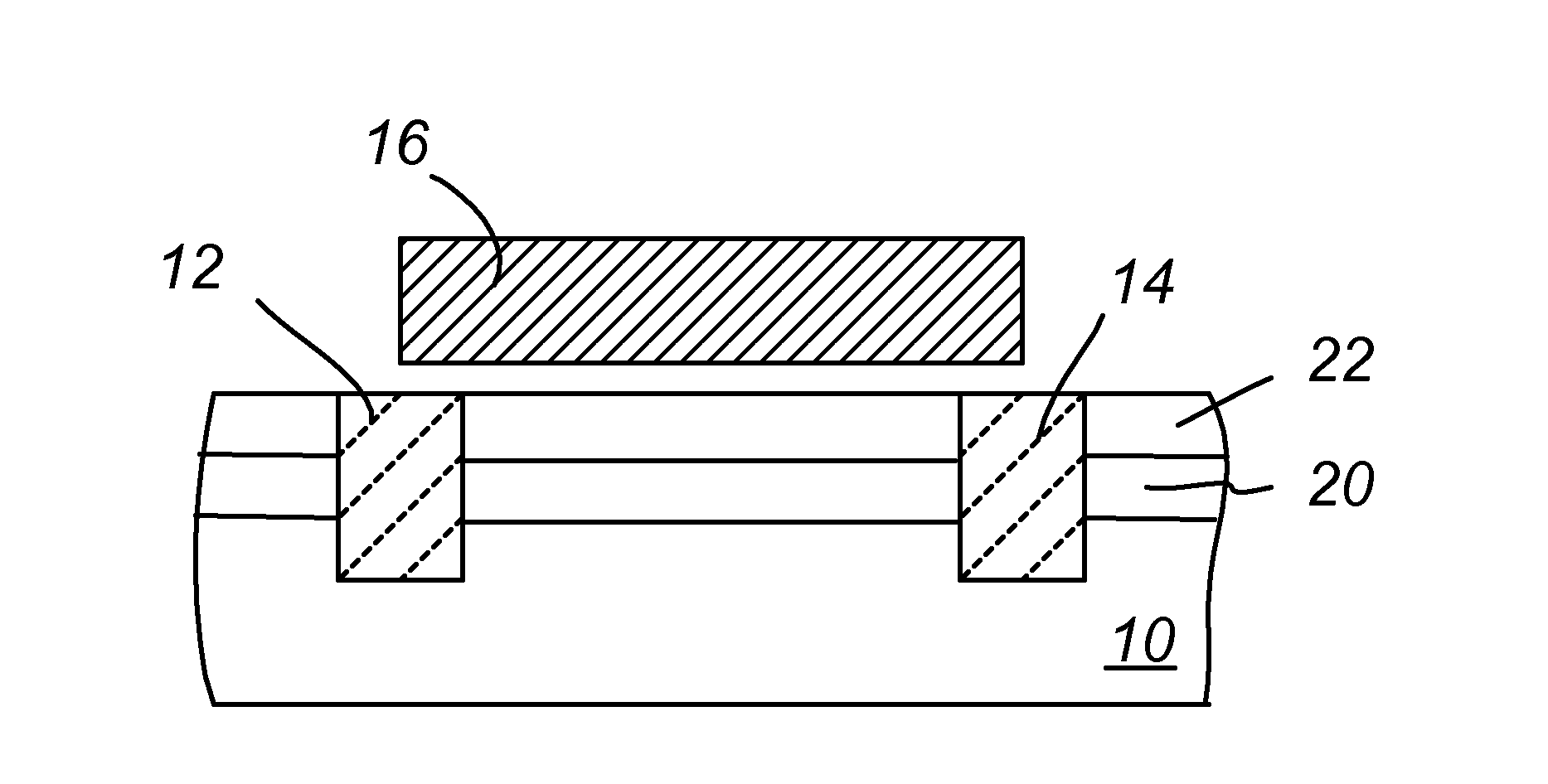
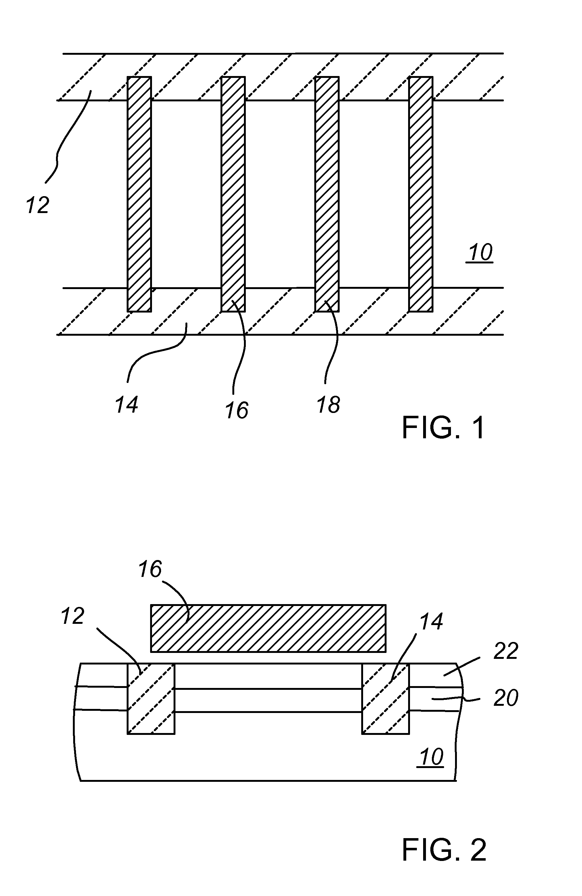
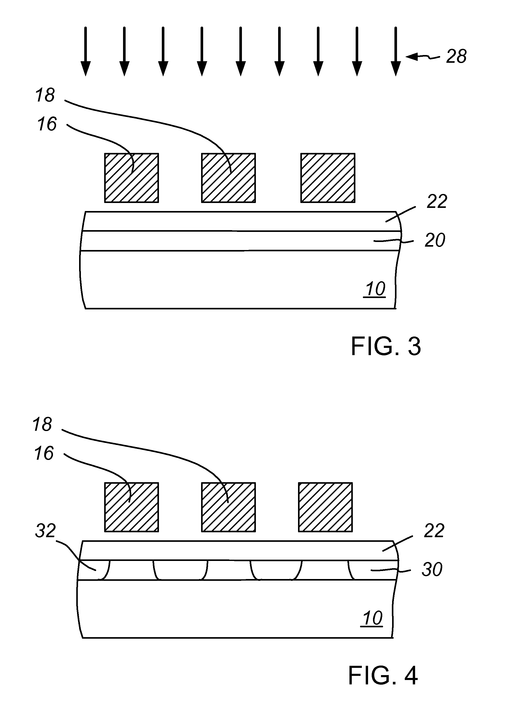
[0011]Aspects of the present invention provide a method of manufacturing a semiconductor device including providing a substrate having a semiconductor surface layer. The substrate has a stressor layer positioned at a depth within the substrate and positioned adjacent the semiconductor surface layer, where the stressor layer is provided in a stressed state in comparison to the semiconductor surface layer. A gate structure is formed above the semiconductor surface layer. A first portion of the stressor layer under the gate structure is relaxed so as to strain a first portion of the semiconductor surface layer under the gate structure, the relaxing accomplished by implanting into second and third portions of the stressor layer aligned with second and third portions of the semiconductor surface layer. The method includes forming respective source and drain regions in at least a part of the second and third portions of the semiconductor surface layer.

[0012]Another aspect of the present i...


PUM


Abstract

Processes for making field effect transistors relax a buried stressor layer to induce strain in a silicon surface layer above the buried stressor layer. The buried stressor layer is relaxed and the surface layer is strained by implantation into at least the buried stressor layer, preferably on both sides of a portion of the surface layer that is to be stressed. For example, implanting ions through the surface silicon layer on either side of the gate structure of the preferred FET implementation into an underlying stressor layer can induce strain in a channel region of the FET. This process can begin with a silicon or silicon-on-insulator substrate with a buried silicon germanium layer having an appropriate thickness and germanium concentration. Other stressor materials can be used.

Description

CROSS REFERENCE TO RELATED APPLICATIONS[0001]This application is a continuation of U.S. application Ser. No. 12 / 768,895, filed Apr. 28, 2010, entitled, “Transistor With Longitudinal Strain In Channel Induced By Buried Stressor Relaxed By Implantation” and incorporated by reference in its entirety.BACKGROUND[0002]1. Field of the Invention[0003]The present invention relates to strained semiconductor devices that incorporate strained active layers and methods for making such devices. The invention more specifically relates to methods of making strained semiconductor devices in which biaxial strain can be provided to the active regions of small geometry devices.[0004]2. Description of the Related Art[0005]Strained silicon is widely viewed as an important technology for obtaining desired advancements in integrated circuit performance. Mobility enhancement results from a combination of reduced effective carrier mass and reduced intervalley (phonon) scattering. For MOS field effect transis...

Claims


Application Information

Patent Timeline
Patent Type & Authority Applications(United States)
IPC IPC(8): H01L29/66
CPCH01L29/66477H01L21/823807H01L21/823814H01L21/823878H01L21/84H01L29/78H01L29/1054
Inventor CLIFTON, PAUL A.
Owner ACORN TECH INC
Why Eureka
Try Eureka