TEM Sample Preparation

a technology of transmission electron microscope and sample preparation, which is applied in the direction of material analysis using wave/particle radiation, instruments, nuclear engineering, etc., can solve the problems of sample bending, overmilling, and other catastrophic defects, and achieve reliable and robust preparation, the effect of removing surface defects

Active Publication Date: 2014-08-07
FEI CO
View PDF0 Cites 7 Cited by
  • Summary
  • Abstract
  • Description
  • Claims
  • Application Information

AI Technical Summary

Benefits of technology

[0010]It is an object of the invention, therefore, to provide an improved method of preparing ultra-thin TEM samples. Preferred embodiments of the present invention combine the current backside thinning process with an additional cleaning step to remove surface defects on the FIB-facing substrate surface. This additional step results in the creation of a cleaned, uniform “hardmask” that controls the ultimate results of the sample thinning, and allows for reliable and robust preparation of samples having thicknesses down to the 10 nm range.

Problems solved by technology

Because a sample must be very thin for viewing with transmission electron microscopy (whether TEM or STEM), preparation of the sample can be delicate, time-consuming work.
Currently thinning below 30 nm is difficult and not robust.
Thickness variations in the sample result in sample bending, overmilling, or other catastrophic defects.
Even though the information that can be discovered by TEM analysis can be very valuable, the entire process of creating and measuring TEM samples has historically been so labor intensive and time consuming that it has not been practical to use this type of analysis for manufacturing process control.
A significant problem for the preparation of ultra thin (<30 nm thick) TEM samples is commonly referred to as “curtaining,” in which non-uniform high-density materials on the surface of an integrated circuit produce a non-planar face on the TEM sample after thinning.
Curtaining artifacts reduce the quality of the TEM imaging and limit the minimal useful specimen thickness.
While this technique works reasonably well for TEM samples having a thickness of 50 to 100 nm, for ultra-thin samples having a sample thickness of 30 nm or less, even samples prepared by inverting the sample before thinning often show milling artifacts resulting in a undesirably non-uniform sample face.

Method used


Image

  • TEM Sample Preparation
  • TEM Sample Preparation
  • TEM Sample Preparation

Examples


Embodiment Construction

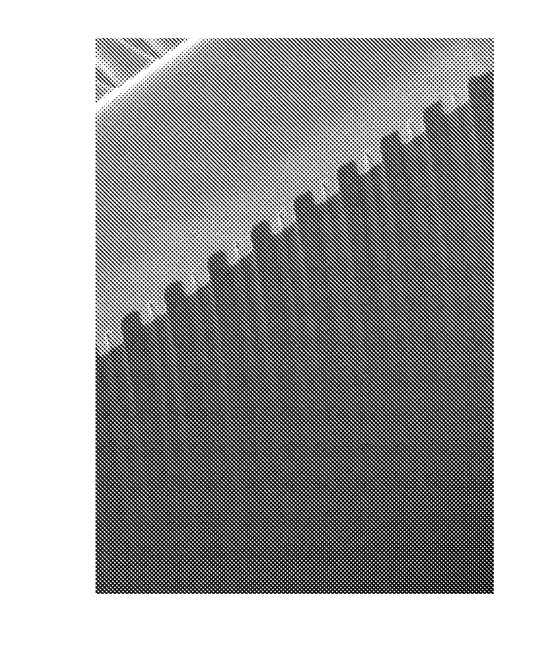
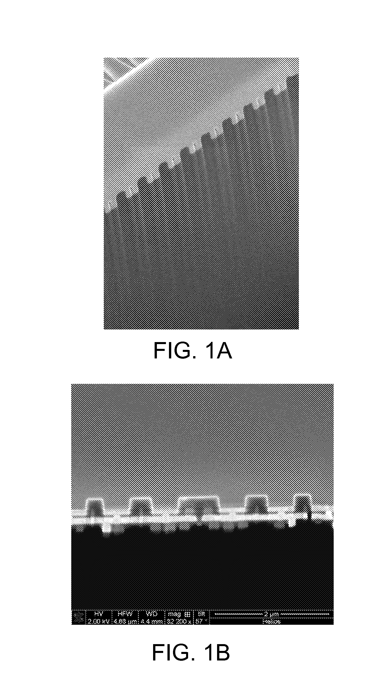
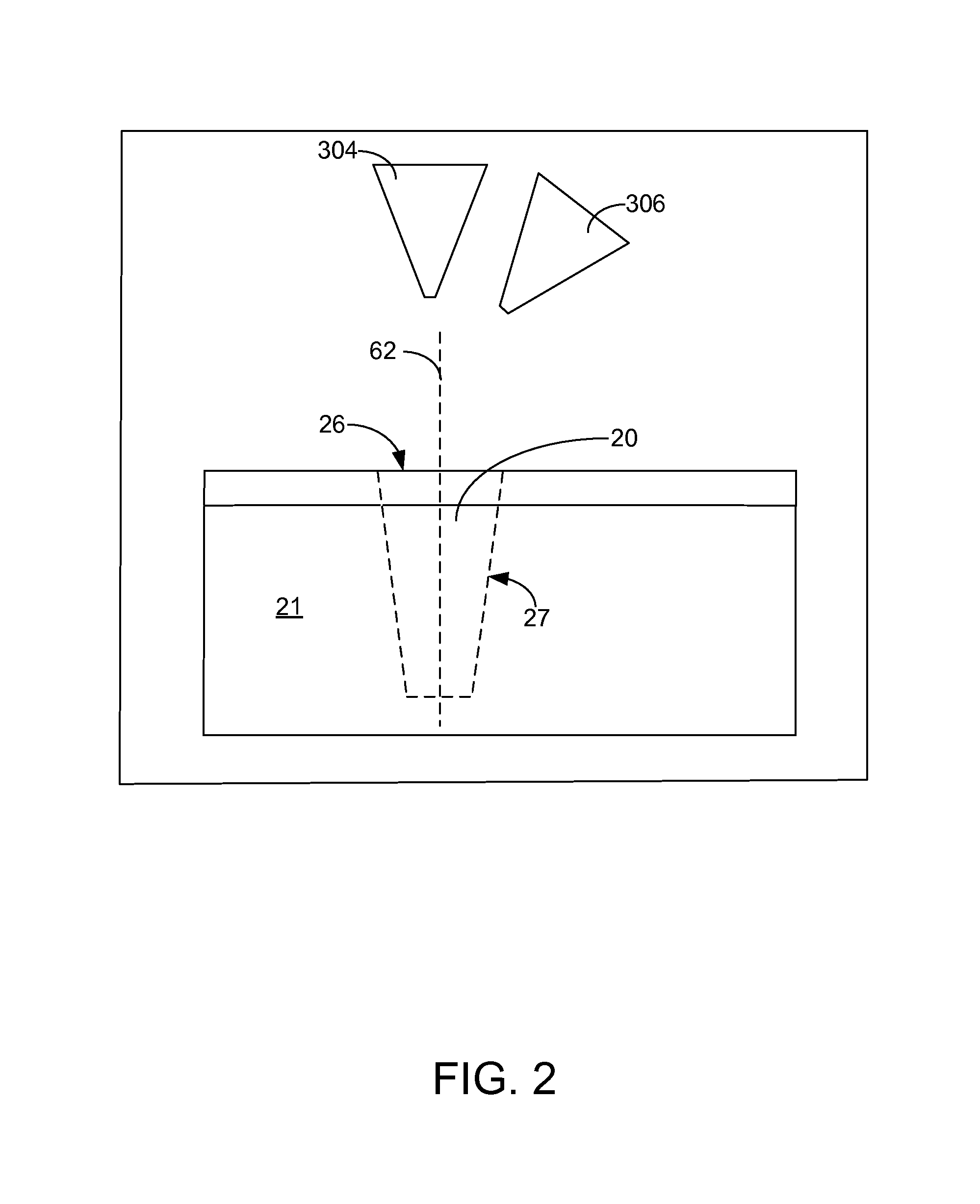
[0029]Preferred embodiments of the present invention are directed at a novel method of preparing ultra-thin TEM samples. Preferred embodiments of the present invention combine the current backside thinning process with an additional cleaning step to remove surface defects on the FIB-facing substrate surface. During the typical TEM sample extraction process, the bottom surface of the sample will accumulate redeposited material from the sample extraction ion milling process. Non-uniformities on the bottom surface can also result from milling artifacts accrued during the bulk material removal process. Applicants have discovered that these material or topographical variations on the surface of the substrate side of the sample have a significant effect upon the TEM sample thinning process. These types of surface variations propagate through the milling process as the TEM sample (also referred to as a lamella) is thinned and result in sidewall non-uniformities that limit the minimum thick...


PUM


Abstract

An improved method of preparing ultra-thin TEM samples that combines backside thinning with an additional cleaning step to remove surface defects on the FIB-facing substrate surface. This additional step results in the creation of a cleaned, uniform “hardmask” that controls the ultimate results of the sample thinning, and allows for reliable and robust preparation of samples having thicknesses down to the 10 nm range.

Description

[0001]This application claims priority from U.S. Provisional Application 61 / 437,474, filed Jan. 28, 2011, which is hereby incorporated by reference.TECHNICAL FIELD OF THE INVENTION[0002]The present invention relates to preparation of samples for transmission electron microscopes and, in particular, to preparation of samples having a thickness of 30 nm or less.BACKGROUND OF THE INVENTION[0003]As semiconductor geometries continue to shrink, manufactures increasingly rely on Transmission electron microscopes (TEMs) for monitoring the process, analyzing defects, and investigating interface layer morphology. Transmission electron microscopes (TEMs) allow observers to see features having sizes on the order of nanometers. In contrast to SEMs, which only image the surface of a material, TEM also allows analysis of the internal structure of a sample. In a TEM, a broad beam impacts the sample and electrons that are transmitted through the sample are focused to form an image of the sample. The...

Claims


Application Information

Patent Timeline
Patent Type & Authority Applications(United States)
IPC IPC(8): H01J37/26
CPCH01J37/261G01N1/286G01N2001/2886H01J2237/31745H01J37/3056
Inventor BLACKWOOD, JEFFREYBRAY, MATTHEWSENOWITZ, COREYBUGGE, CLIFF
Owner FEI CO
Why Eureka
Try Eureka