Silicon carbide semiconductor device and manufacturing method for same

a technology of silicon carbide and semiconductor devices, which is applied in the direction of semiconductor devices, basic electric elements, electrical equipment, etc., can solve the problems of increasing the likelihood of crystal growth irregularities, crystal mixtures of different polytypes are unavoidable, and crystal defects such as dislocations are likely to occur, so as to achieve outstanding electrical characteristics and eliminate surface defects

Inactive Publication Date: 2016-09-01
FUJI ELECTRIC CO LTD
View PDF4 Cites 7 Cited by
  • Summary
  • Abstract
  • Description
  • Claims
  • Application Information

AI Technical Summary

Benefits of technology

[0040]According to the present invention, surface defects can be eliminated by introducing strain energy to either the underlying substrate or the epitaxial layer of the silicon carbide semiconductor to form a strain layer, and recrystallizing the strain layer using heat treatment, thereby making it possible to obtain a crystal defect free device formation region, and to provide a silicon carbide semiconductor having outstanding electrical characteristics.

Problems solved by technology

These outstanding physical characteristics are a function of the interatomic bond energy of Si and C as being high; however, a problem is that the differences in the periodic structures of Si and C at bonding time result in an abundance of polytypes (crystal polymorphs), such as 2H, 3C, 4H, 6H, and 15R in the crystal, increasing the likelihood of the generation of irregularities during crystal growth.
Therefore, a crystal mixture of different polytypes is unavoidable when fabricating a SiC single crystal, and the reality is that crystal defects such as dislocations are likely to occur due to crystal irregularities arising from the formation of polytype crystals.
Therefore, an incredibly larger number of crystal defects are found in current SiC semiconductors than in Si semiconductors, which are nearly devoid of dislocations.
It should be noted that because molten SiC is not very stable at high temperatures, a SiC crystal ingot, which is the raw material for a SiC substrate, is difficult to grow from a melt in the same way as Si, and the SiC ingot is generally fabricated using a sublimation technique.
For example, in a device such as a SiC-Schottky barrier diode (SiC-SBD) or SiC-MOSFET in particular, because a crystal defect in the surface of the SiC epilayer thereof is directly linked to characteristics degradation, and reliability and quality, reductions in the density of surface defects and the establishment of a method for evaluating surface defect density are important challenges for improving the non-defective rate and reliability of SiC devices.
Defects extending into and penetrating through the epilayer in succession to dislocation defects such as the aforementioned TSDs and TEDs generated in the SiC underlying substrate are currently still not under full control; in particular, it is practically impossible to control carrot-type defects, which form uneven patterns on a surface.
These defects are known to be associated with poor electrical characteristics in devices, especially unfavorable leakage current, and are the main cause of drops in the non-defective rate of products.
In the SiC-SBD device fabrication processes explained above, when crystal defects exist in the surface of the SiC epilayer 2 formed using step (b), the formation of a good Schottky junction is impeded when the Ti silicide is formed in step (d), which results in poorer SBD device characteristics.
There is a high risk of SiC epilayer surface defects affecting the quality of the front surface side silicide layer that form the SBD Schottky barrier and / or the MOSFET gate oxide film.
In particular, in the SBD, there is the likelihood of the height of the Schottky barrier changing and leakage current increasing in accordance with the generation of defects.
Because these surface defects tend to produce step-shaped height differences in the SiC surface, there is also the likelihood of the formation of the silicide layer becoming nonuniform due to these steps, resulting in electric-field concentration points localized.

Method used


Image

  • Silicon carbide semiconductor device and manufacturing method for same
  • Silicon carbide semiconductor device and manufacturing method for same
  • Silicon carbide semiconductor device and manufacturing method for same

Examples


example 1

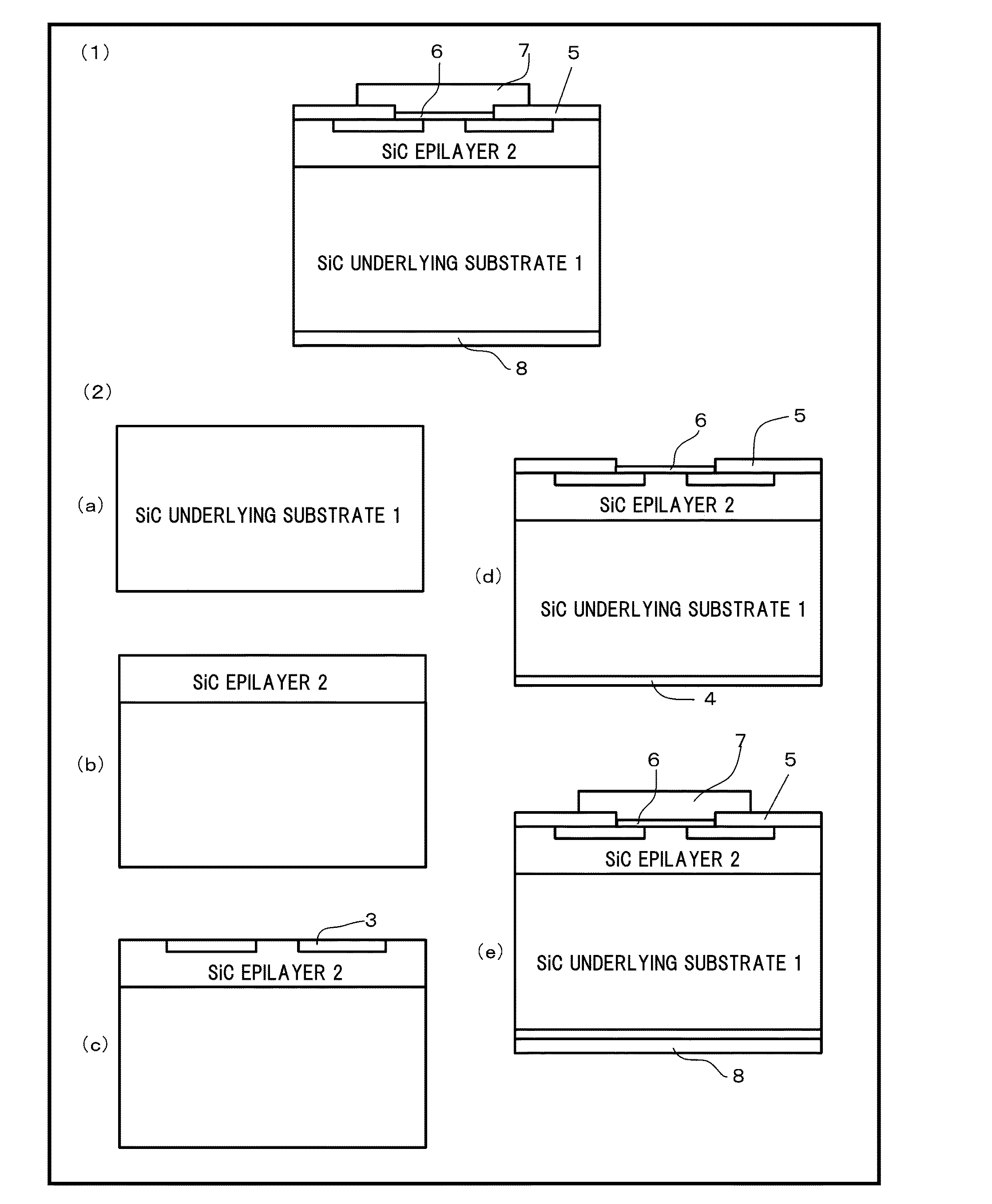
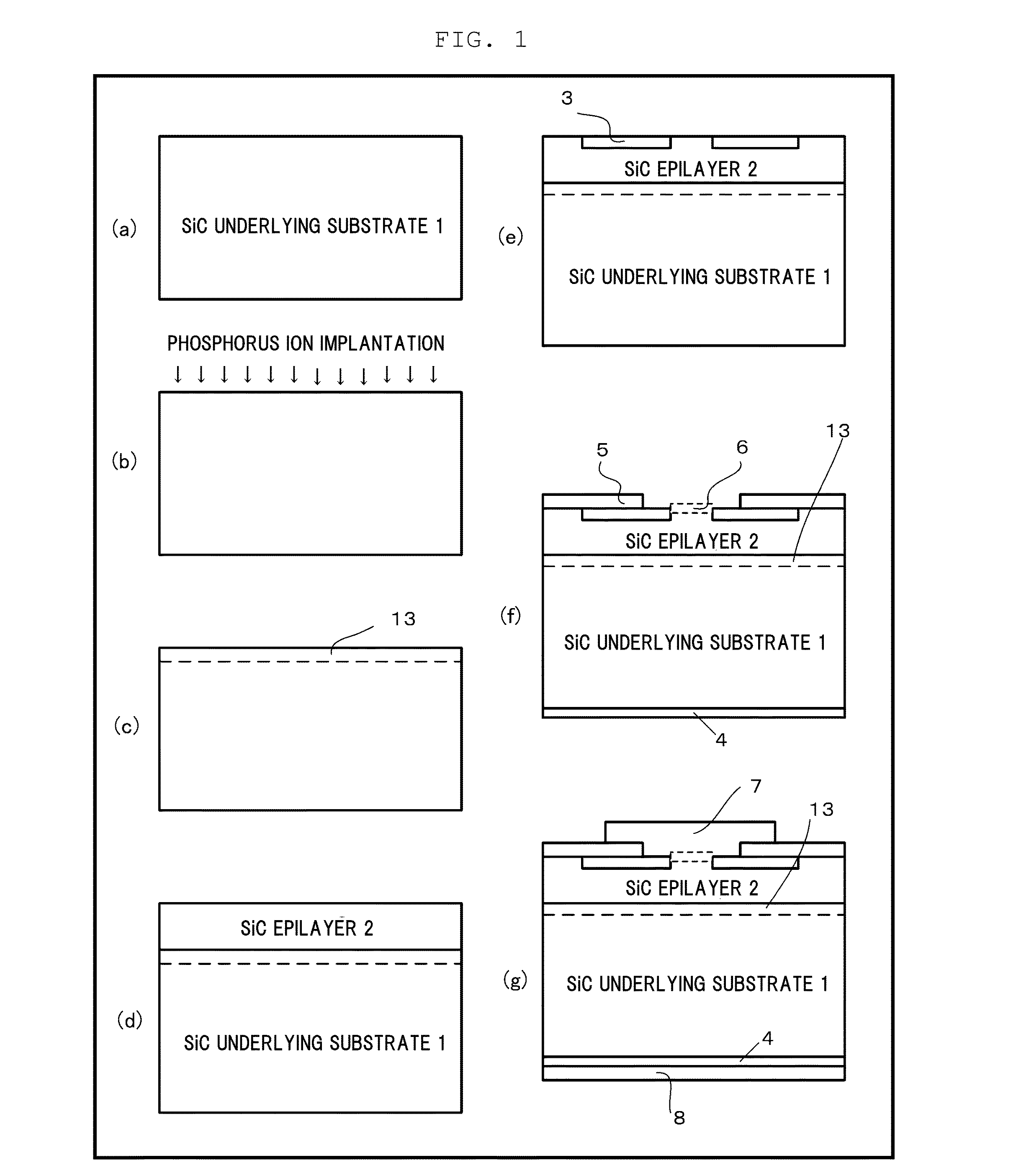
[0071]SiC-SBD was fabricated in accordance with the manufacturing process shown in FIG. 1.

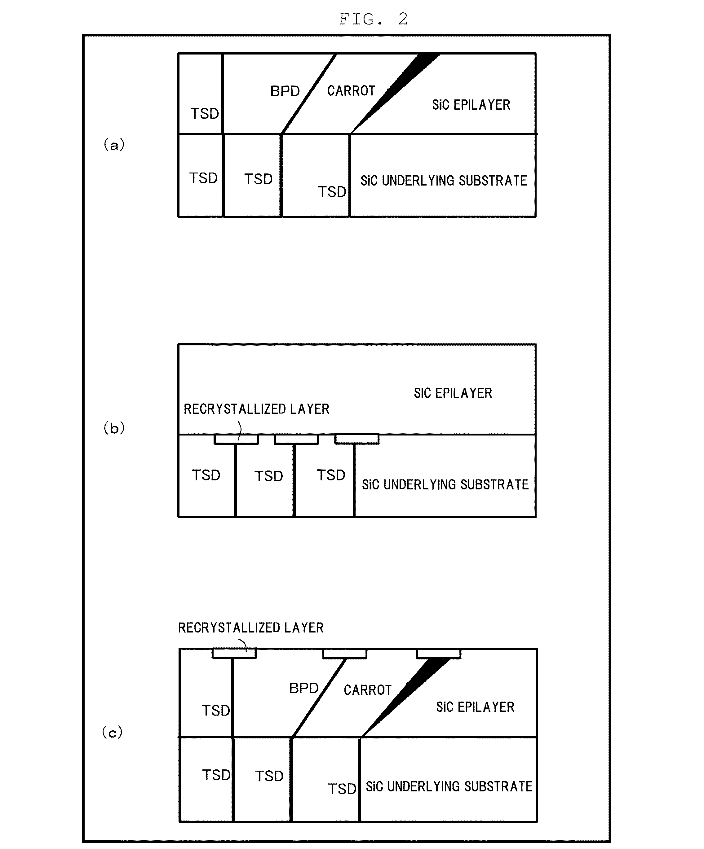
[0072]As step (b), phosphorus was implanted over the entire Si surface of the SiC underlying substrate 1 in two stages to form an ion implantation region (strain layer). At this point, first stage implantation was performed at a dosage of 2×1015 cm−2 and an accelerating energy of 250 keV, and second stage implantation was performed at a dosage of 5×1014 cm−2 and an accelerating energy of 70 keV. Implantation was performed at room temperature. Next, as step (c), heat treatment using high-frequency induction heating was performed at a temperature of 1600° C. for 180 seconds under a normal pressure Ar environment, and the ion implantation region (strain layer) introduced in step (b) was recrystallized to form the recrystallized layer 13 (the heat treatment at 1600° C. for 180 seconds may be substituted with a heat treatment at 2000° C. for 30 seconds). Although not shown in the drawing, a carbon f...

example 2

[0076]An SiC-SBD was fabricated in accordance with the manufacturing processes shown in FIG. 4.

[0077]As step (b), an n−-type SiC epilayer 2 (1×1016 cm−3, 10 μm) was formed on the Si surface of the SiC underlying substrate 1 (a buffer layer (1×1018 cm−3, 0.5 μm) may be formed here prior to forming the n−-type SiC epilayer 2). An inspection was performed using a surface defect evaluation apparatus subsequent to forming the n-SiC epilayer 2, and four defects / cm2 were detected.

[0078]Next, ion implantation of Al was performed in three stages using an oxide film mask (not shown) formed on the surface of the SiC epilayer 2 by photoetching to form a voltage withstanding structure part. The p-type regions 3 were formed by performing ion implantation in sequence having as implantation conditions 5×1012 cm−2 / 350 keV in the first stage, 3×1012 cm−2 / 150 keV in the second stage, and 2×1012 cm−2 / 100 keV in the third stage. The implantation temperature was 500° C. Next, as step (d), after forming a...


PUM

PropertyMeasurementUnit
temperatureaaaaaaaaaa
thicknessaaaaaaaaaa
resistivityaaaaaaaaaa

Abstract

A method of manufacturing a silicon carbide semiconductor device in which a first-conductivity-type silicon carbide semiconductor epitaxial layer is formed on a main surface of a first-conductivity-type silicon carbide semiconductor substrate, wherein the silicon carbide semiconductor device manufacturing method includes: a step for supplying strain energy to at least one of (i) a surface layer of the surface of the silicon carbide semiconductor substrate on which the silicon carbide semiconductor epitaxial layer is formed, and (ii) the surface of the silicon carbide semiconductor epitaxial layer, a step for forming a carbon film on the surface layer, and a step for forming a recrystallized layer by adding a heat treatment for recrystallizing the surface layer to which the strain energy is supplied.

Description

TECHNICAL FIELD[0001]The present invention relates to a silicon carbide semiconductor device and a method for manufacturing same related to the reduction of the density of crystal defects in the surface of a silicon carbide epitaxial layer.BACKGROUND ART[0002]In recent years, attention has focused on silicon carbide semiconductor devices as devices capable of overcoming limitations in silicon device characteristics. In particular, silicon carbide semiconductor devices are expected to find applications in power semiconductor devices by making the most of such outstanding physical characteristics as a higher breakdown electric field strength (roughly 10 times higher) and higher thermal conductivity (roughly 3 times higher) than silicon semiconductor devices.[0003]These outstanding physical characteristics are a function of the interatomic bond energy of Si and C as being high; however, a problem is that the differences in the periodic structures of Si and C at bonding time result in a...

Claims


Application Information

Patent Timeline
Patent Type & Authority Applications(United States)
IPC IPC(8): H01L21/02H01L21/04H01L29/66H01L29/16H01L29/32H01L29/47H01L29/872H01L21/265
CPCH01L21/02529H01L29/872H01L21/02378H01L21/02689H01L21/046H01L29/6606H01L21/26506H01L29/1608H01L29/32H01L29/47H01L21/0495H01L21/02675H01L29/0619
Inventor KITAMURA, SHOJI
Owner FUJI ELECTRIC CO LTD
Why Eureka
Try Eureka