Shift register circuit and shading waveform generating method

a shift register and shading waveform technology, applied in static storage, digital storage, instruments, etc., can solve the problems of inability to implement additional gate driving circuits independently, inconsistency of charging voltage of pixel units, flickering problem on display panels, etc., to achieve efficient shading on output signals and efficiently form shading waveforms

Active Publication Date: 2014-08-07
AU OPTRONICS CORP
View PDF15 Cites 31 Cited by
  • Summary
  • Abstract
  • Description
  • Claims
  • Application Information

AI Technical Summary

Benefits of technology

[0009]In order to solve the aforesaid problem and form a shading waveform efficiently, the invention provides a gate-shading circuit in a shift register, wherein the gate-shading circuit of each stage of the shift register includes a plurality of switches. When the aforesaid switches are turned on, voltages on a gate terminal and an output terminal of an output transistor in the shift register can be pulled down respectively. The output transistor can be turned off gradually by pulling down the voltage on the gate terminal so as to change

Problems solved by technology

Accordingly, the gate driving signal will be distorted gradually, which may cause an inconsistency of charging voltages of pixel units at different positions (on the same row/column).
The inconsistency

Method used


Image

  • Shift register circuit and shading waveform generating method
  • Shift register circuit and shading waveform generating method
  • Shift register circuit and shading waveform generating method

Examples


Embodiment Construction

[0022]A plurality of embodiments of the invention will be disclosed below with reference to drawings. For purpose of clear description, many details in practice will be described together with the following description. However, it should be understood that these details in practice are not used to limit the invention. In some embodiments of the invention, these details in practice are unnecessary. Additionally, for purpose of simplifying the drawings, some conventional and common structures and components in the drawings will be illustrated in a simple and schematic manner.

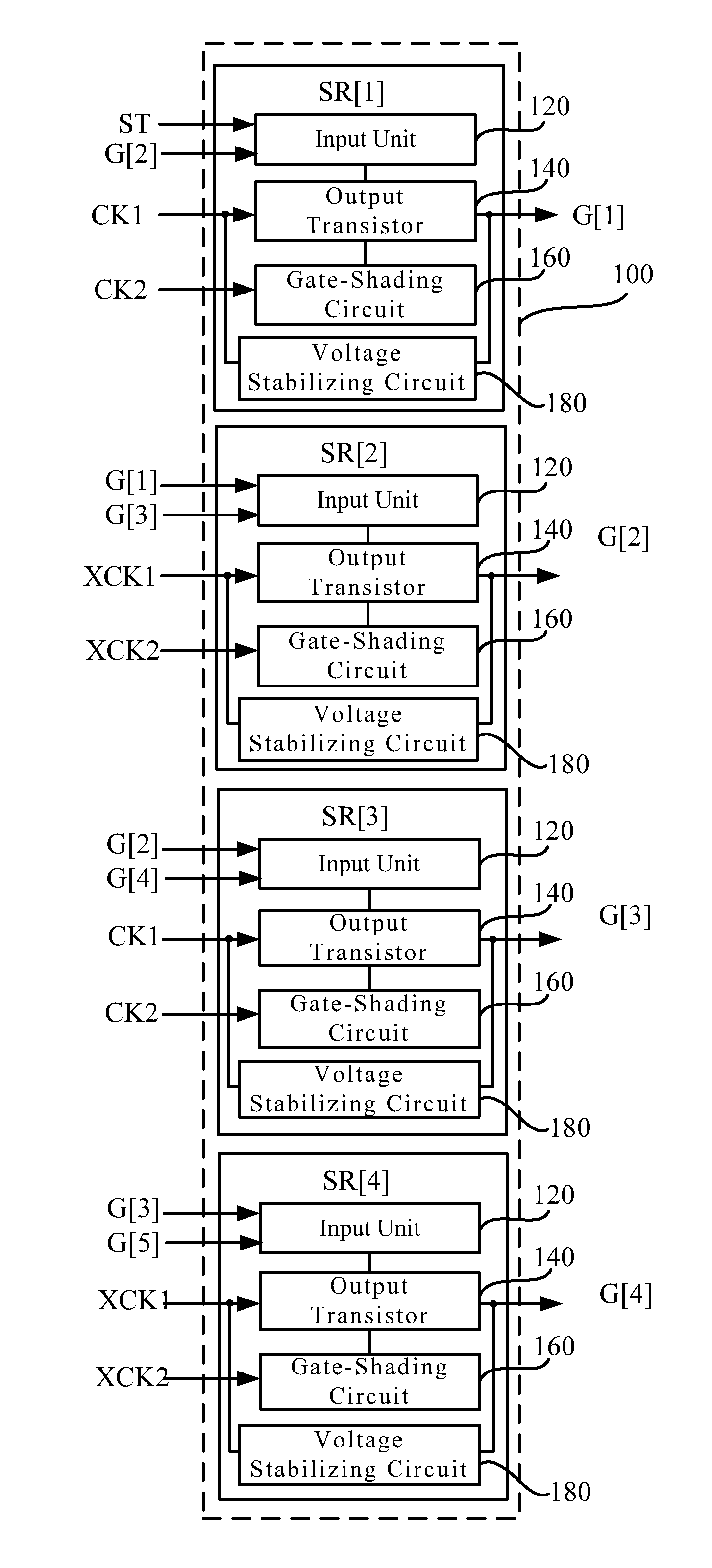
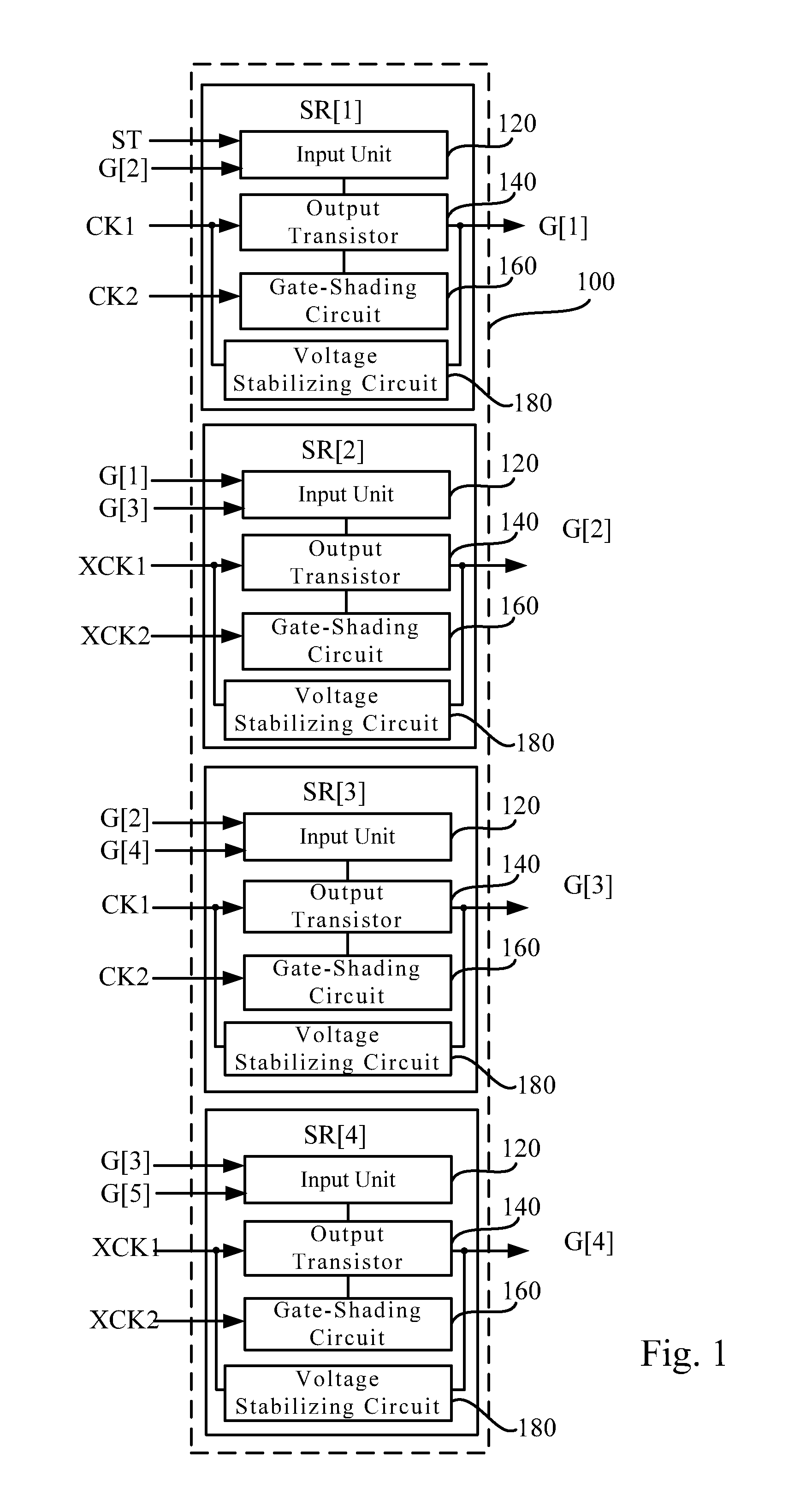
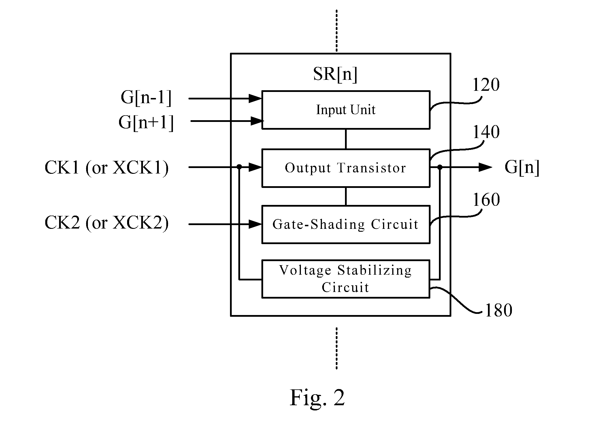
[0023]Referring to FIG. 1, it illustrates a schematic view of a shift register circuit 100 according to an embodiment of the invention. The shift register circuit 100 includes a plurality of stages of shift registers. For example, in the embodiment as shown in FIG. 1, the shift register circuit 100 includes multiple stages of shift registers, such as shift registers SR[1], SR[2] and SR[3]. In an example of practi...


PUM


Abstract

A shift register circuit and a shading waveform generating method are disclosed. The shift register circuit includes plural stages of shift registers. Each stage of the shift register includes an output transistor, an input unit and a gate-shading circuit. The output transistor is configured for generating an output signal of the stage of the shift register. The input unit is configured for controlling a voltage level on a gate terminal of the output transistor. The gate-shading circuit includes a first switch, a second switch and a third switch. The first switch is configured for outputting a control signal. The second switch is configured for pulling down the voltage level on the gate terminal of the output transistor according to the control signal. The third switch is configured for pulling down a level on an output terminal of the output transistor according to the control signal.

Description

RELATED APPLICATIONS[0001]This application claims priority to Taiwan Application Serial Number 102104907, filed Feb. 7, 2013, which is herein incorporated by reference.BACKGROUND[0002]1. Field of Invention[0003]The invention relates to a circuit structure in a display. More particularly, the invention relates to a shift register circuit configured in a display, which can generate a shading waveform.[0004]2. Description of Related Art[0005]In a conventional liquid crystal display, data lines and scan lines perpendicularly go across each others and form a pixel matrix. Scan lines, which are electrically coupled to gates of display transistors in the liquid crystal display, are configured for controlling switching states of display transistors, so as to determine whether to write image signals into the display transistors or not.[0006]When liquid crystal units arranged in the pixel matrix are charged, a gate driving signal will be influenced by varied impedances, which vary correspondi...

Claims


Application Information

Patent Timeline
IPC IPC(8): G11C19/28
CPCG11C19/28G09G3/3677G09G2310/0286
Inventor CHIEN, LING-YINGLIU, KUANG-HSIANGTING, YU-HSIN
Owner AU OPTRONICS CORP
Why Eureka
Try Eureka